Semiconductor integrated circuit interlinkage structure interstitial copper-plating method and structure

A technology of interconnection structure and integrated circuit, which is applied in semiconductor/solid-state device manufacturing, circuits, electrical components, etc., can solve problems such as poor gap filling characteristics and gaps, and achieve the effect of improving device yield

Inactive Publication Date: 2010-04-07
SEMICON MFG INT (SHANGHAI) CORP +1
View PDF7 Cites 0 Cited by
  • Summary
  • Abstract
  • Description
  • Claims
  • Application Information

AI Technical Summary

Problems solved by technology

As devices become smaller and integration requirements increase, limitations in copper and low-k dielectric materials include poor interstitial properties in copper films, which can lead to voids and other undesirable structures

Method used


Image

  • Semiconductor integrated circuit interlinkage structure interstitial copper-plating method and structure
  • Semiconductor integrated circuit interlinkage structure interstitial copper-plating method and structure
  • Semiconductor integrated circuit interlinkage structure interstitial copper-plating method and structure

Examples


Embodiment Construction

[0014] According to the present invention, techniques for fabricating integrated circuits are provided. More specifically, the present invention provides methods and devices for fabricating metal interconnect structures with improved interstitial properties. By way of example only, the invention has been applied to copper metal structures, such as dual damascene structures for advanced signal processing devices. It should be recognized, however, that the invention has broader applicability. For example, the invention may be applied to microprocessor devices, memory devices, application specific integrated circuit devices, and various other interconnect structures.

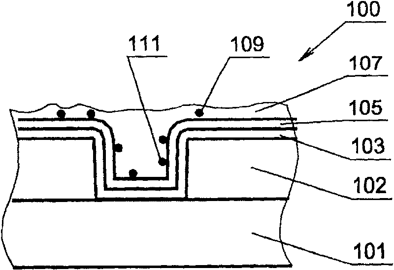
[0015] figure 1 is a simplified cross-sectional view of the interconnect structure of a conventional copper interconnect. As shown, device 100 includes a substrate 101, which is a silicon substrate. Above the substrate is an interlayer dielectric layer 102 . A contact structure is formed inside the dielectric ...


PUM


Abstract

The invention relates to a method of integrated circuit apparatus using to form a comprising interconnection structure (such as copper double metal mounting). The method comprises and provides a substrate and a middle dielectric layer is formed and covered on the substrate. The method is also comprises a nano-pattern middle dielectric later to form a contacting structure and a cutoff metal layer is formed and covered on the contacting structure. The method comprises the following processes: a seed layer is formed and covered on the cutoff metal layer and an oxygen substance is used for processing the seed layer as well as a desired thickness of an oxidation layer is formed on the seed layer. When a transfer is carried out from the step of effecting on the seed layer in the substrate, the method uses the oxidation layer to protect the seed layer and prevent seed layer from the contamination, as well as the liquid copper-containing material is contacted and covered on the oxidation layerto solute the oxidation layer. At the same time, a certain thickness of copper-containing material is formed using a copper-plated process to start fill the contacting structure.

Description

technical field [0001] The present invention relates generally to integrated circuits and integrated circuit processing methods for fabricating electronic devices. More particularly, the present invention relates to methods and devices for fabricating metal interconnect structures with improved interstitial properties. Background technique [0002] The present invention relates to an integrated circuit and a processing method for manufacturing a semiconductor device. More specifically, the present invention provides a method and device for fabricating metal interconnect structures with improved interstitial properties. By way of example only, the invention has been applied to copper metal structures, such as dual damascene structures for advanced signal processing devices. It should be recognized, however, that the invention has broader applicability. For example, the invention may be applied to microprocessor devices, memory devices, application specific integrated circu...

Claims


Application Information

Patent Timeline
Patent Type & Authority Patents(China)
IPC IPC(8): H01L21/768
Inventor 向阳辉姜庆堂
Owner SEMICON MFG INT (SHANGHAI) CORP
Why Eureka
Try Eureka