Supercharge Your Innovation With Domain-Expert AI Agents!

Semiconductor device and fabrication method thereof

A semiconductor and insulating layer technology, which is applied in semiconductor/solid-state device manufacturing, semiconductor devices, semiconductor/solid-state device components, etc., can solve problems such as bubbles, metals or oxides, and corrosion

Inactive Publication Date: 2008-07-02
DONGBU HITEK CO LTD
View PDF0 Cites 1 Cited by
  • Summary
  • Abstract
  • Description
  • Claims
  • Application Information

AI Technical Summary

Problems solved by technology

HF causes problems of generating bubbles in the insulating layer 12 or causes corrosion in metals or oxides

Method used


Image

  • Semiconductor device and fabrication method thereof
  • Semiconductor device and fabrication method thereof

Examples


Embodiment Construction

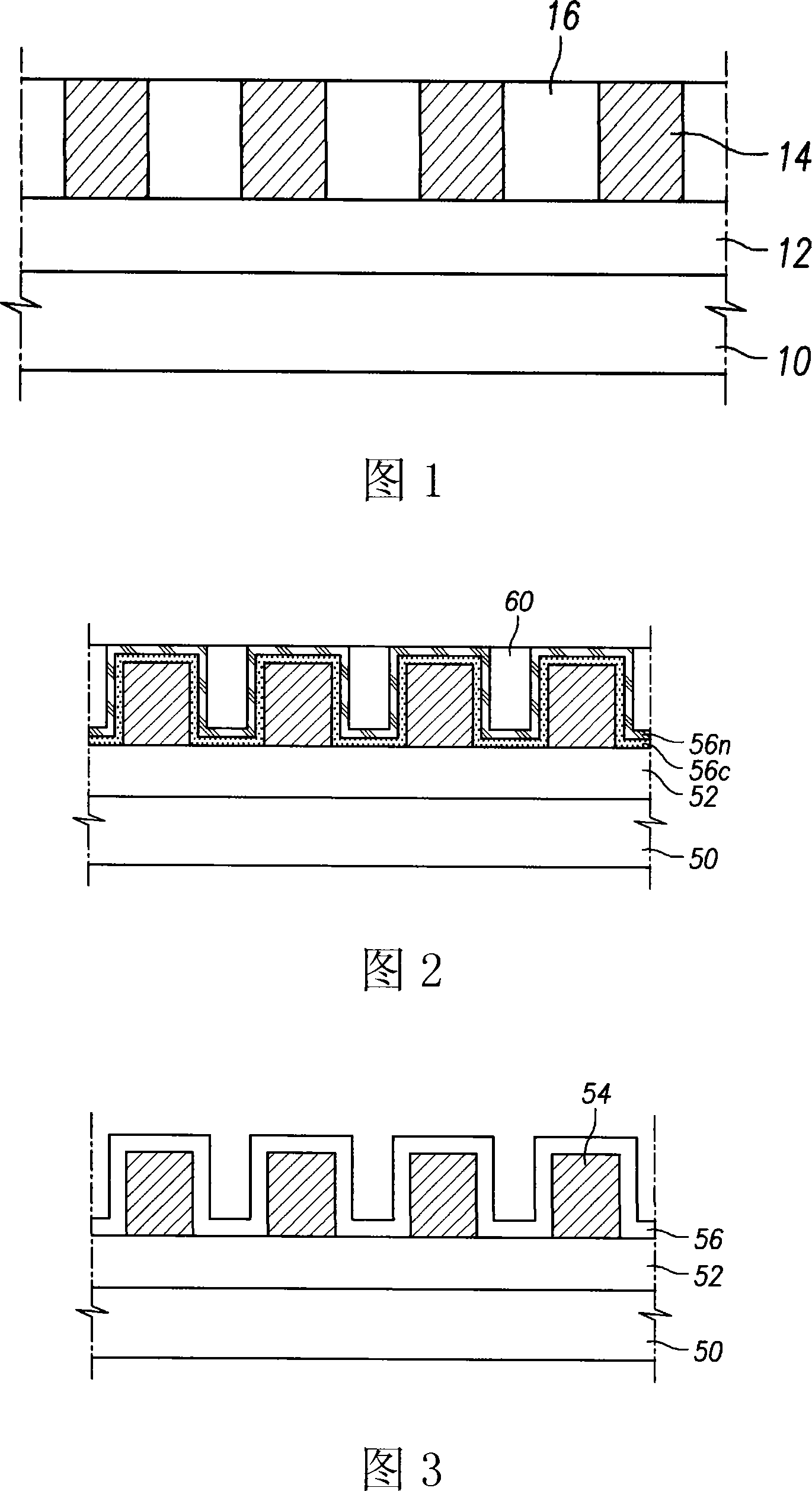
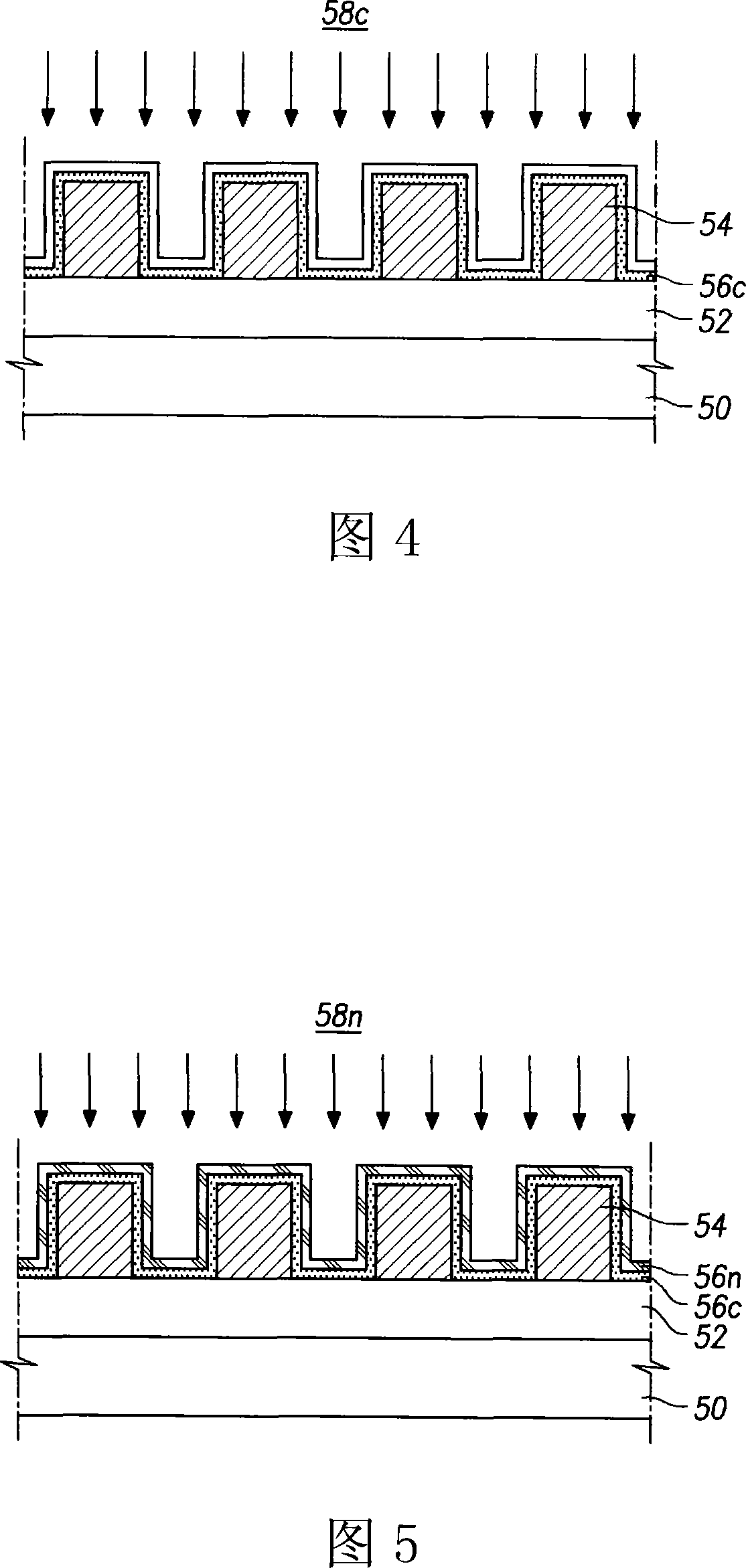
[0015] As shown in the embodiments of FIGS. 2 and 3 , first insulating layer 52 can be formed on and / or over semiconductor substrate 50 . Subsequently, a wire layer having a plurality of wire patterns 54 can be formed on and / or over first insulating layer 52 . The first insulating layer 52 can be used as an interlayer insulating layer to electrically insulate the lower structure from the wiring layer or the covering layer of the gate below the wiring layer.

[0016] The space gap between the respective line patterns 54 can be reduced corresponding to a highly integrated semiconductor device. In a highly integrated semiconductor device requiring a fast operating speed, it is necessary to minimize the parasitic capacitance between the line patterns 54 . To this end, electrical insulation and planarization of the line pattern 54 may be performed. For multiple wire layers, spatial gaps between the wire patterns 54 may be filled with the second insulating layer 60 serving as an i...


PUM


Abstract

A semiconductor device including a first insulating layer having a hydroxyl radical formed over a semiconductor substrate; a line layer having a plurality of line patterns formed over the first insulating layer, the plurality if line patterns being arranged such that a spatial gap is provided therebetween; a fluorine-doped second insulating layer formed in the spatial gap between respective line patterns; and a multilayered diffusion prevention layer including a first oxide layer for suppressing an increase of a dielectric constant between the plurality of line patterns and a second oxide layer for preventing the diffusion of fluorine from the fluorine-doped second insulating layer into the first insulating layer.

Description

[0001] This application claims the benefit of Korean Patent Application No. 10-2006-0137359 filed on December 29, 2006, the entire contents of which are hereby incorporated by reference. technical field [0002] The present invention relates to a semiconductor device and a manufacturing method thereof, and more particularly to a semiconductor device having a fluorine-doped insulating layer and a manufacturing method thereof. Background technique [0003] A semiconductor device may have a highly integrated structure including line layers with spatial gaps. However, such devices exhibit increased parasitic capacitance, causing delays in signal transfer and also signal interference. [0004] To alleviate such problems, semiconductor devices may incorporate low-k dielectrics as interlayer insulating layers to fill space gaps between line patterns and insulating layers. A fluorine-doped oxide layer can be used as an insulating layer. Fluorine-doped oxide layers can have good pr...

Claims


Application Information

Patent Timeline
IPC IPC(8): H01L23/532H01L21/768H01L21/31
CPCH01L2924/0002H01L23/53295H01L21/76834H01L23/5329H01L21/76832H01L23/5222H01L2924/00H01L21/28
Inventor 黄宗泽
Owner DONGBU HITEK CO LTD
Features
  • R&D
  • Intellectual Property
  • Life Sciences
  • Materials
  • Tech Scout
  • Unparalleled Data Quality
  • Higher Quality Content
  • 60% Fewer Hallucinations
Learn More