A transmission electron microscope measurement support grid based on phase change materials

A phase change material and electrical technology, applied in measurement devices, analytical materials, material analysis using wave/particle radiation, etc. The electrode position cannot be changed, and the direct measurement is difficult to achieve the effect of selective measurement, reliable performance and simple structure.

Inactive Publication Date: 2008-07-09
BEIJING UNIV OF TECH
View PDF0 Cites 12 Cited by
  • Summary
  • Abstract
  • Description
  • Claims
  • Application Information

AI Technical Summary

Problems solved by technology

With the development of microelectromechanical systems (MEMS, micro electromechanical system) and nanoelectromechanical systems (NEMS, nanoelectromechanical system), it is particularly urgent to study the electrical properties of single nanowires or nanoscale microdevices under the action of an electric field, but Due to the small structure of a single nanowire or micro-device, it is difficult to manipulate, how to fix and apply an electric field to a single nanowire or micro-device sample in a transmission electron microscope, to reveal the electrical properties of nanomaterials under the action of an external electric field from the nanoscale and atomic level performance, and the electric field effect becomes a difficult problem for researchers
At present, due to the extremely limited space between the sample stage and the pole piece in the transmission electron microscope, generally 1-3mm, it is very difficult to directly measure the mechanical properties of a single nanowire or nanofilm at atomic scale resolution. The method of electrical measurement of nanowires that has been reported in is mainly based on the focused ion beam FIB (focus iron beam) technology, depositing electrodes at both ends of the object to be tested for measurement, but once the circuit is built, the length of the nanowires between the electrodes And the position of the electrode cannot be changed, and the electrical behavior of the sample to be tested under the action of an electric field and the change of the atomic-scale microstructure cannot be directly observed under the transmission electron microscope

Method used


Image

  • A transmission electron microscope measurement support grid based on phase change materials

Examples


Embodiment Construction

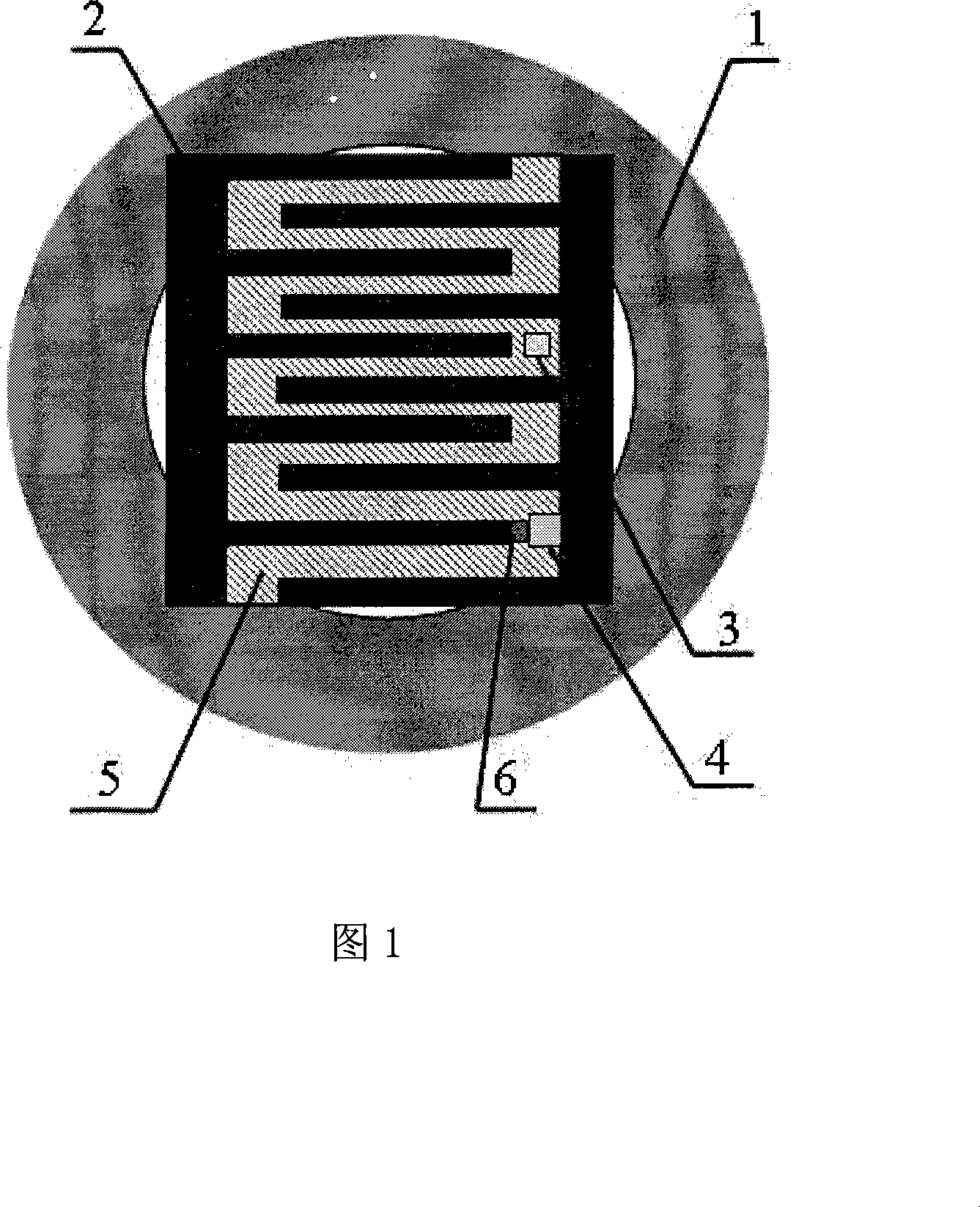
[0018] This embodiment will be described in detail below in conjunction with FIG. 1 .

[0019] This embodiment includes a support part and a circuit part, the support part is a metal ring 1, the circuit part includes two opposite metal electrodes 2 and the elements to be measured 3, 4 and phase change material film 5 therebetween, the electrodes 2 and the metal The ring 1 is insulated and bonded, the phase change material film 5 is amorphous, the device to be tested 3 is located on the film 5 but has no contact with the electrodes, and the device to be tested 4 is integrated on one of the electrodes. Two electrodes 2 are symmetrically distributed in the center of the metal ring 1 .

[0020] In this embodiment, two electrodes 2 are insulated and fixed on the copper ring of a transmission electron microscope commonly used, and a layer of phase-change material amorphous film 5 is laid between the two electrodes 2. The electron beam can induce the crystallization of the phase-chan...


PUM

PropertyMeasurementUnit
thicknessaaaaaaaaaa
widthaaaaaaaaaa
lengthaaaaaaaaaa

Abstract

The invention relates to a transmission electron microscope sample loading net, which pertains to the measurement field of nano-materials. The invention includes a support part and a circuit part, the support part includes a metal ring (1), the circuit part includes two electrodes (2), an element which is ready to be measured and a phase change material amorphous thin film (5), the electrodes (2) are insulatedly bonded with the metal ring (1), the phase change material amorphous thin film (5) is evenly distributed between the two electrodes (2), the phase change material thin film (5) is amorphous, the element which is ready to be measured is positioned in the phase change material amorphous thin film (5) or is integrated on one electrode (2). The connection lines in the invention are characterized by erasable property, the higher voltage is added on the both ends of the electrodes, or the loading net is directly done with certain laser pulse irradiation, so the phase change material thin film is completely amorphous, the formed current path disappears, the optional and repeated erasable properties of the measurement circuit are realized.

Description

technical field [0001] The invention relates to a transmission electron microscope sample carrying net, which belongs to the field of nanometer material measurement. Background technique [0002] Transmission electron microscope (hereinafter referred to as transmission electron microscope or electron microscope) is a modern large-scale instrument and a powerful tool for studying the microstructure of matter. It has a wide range of applications in physics, chemistry, material science, life science and other fields, especially the rapidly developing In the field of nano science and technology, it is one of the most powerful research tools. At present, the resolution of the transmission electron microscope has reached 0.2nm, which is close to the atomic distance of solid matter. With the development of microelectromechanical systems (MEMS, micro electromechanical system) and nanoelectromechanical systems (NEMS, nanoelectromechanical system), it is particularly urgent to study t...

Claims


Application Information

Patent Timeline
Patent Type & Authority Applications(China)
IPC IPC(8): H01J37/20H01J37/26G01N23/00
Inventor 张泽王珂刘攀韩晓东
Owner BEIJING UNIV OF TECH
Why Eureka
Try Eureka