Thin-film transistor, active element array substrate as well as liquid crystal display panel

A technology for liquid crystal display panels and thin film transistors, applied in transistors, electrical components, electrical solid devices, etc., can solve the problems affecting the characteristics of thin film transistor components, disconnection of scanning lines or data lines, and increase in wiring impedance, so as to maintain display quality. Effect

Inactive Publication Date: 2008-07-23
AU OPTRONICS CORP
View PDF0 Cites 18 Cited by
  • Summary
  • Abstract
  • Description
  • Claims
  • Application Information

AI Technical Summary

Problems solved by technology

However, since the etching rate of the etching solution to molybdenum is greater than that of the etching solution to aluminum, the etching solution tends to cause an undercut 110 (undercut) phenomenon as shown in FIG. 1 to the first molybdenum layer 102
In this way, when the electrode in the thin film transistor adopts the structure of molybdenum layer / aluminum layer / molybdenum layer, the above-mentioned undercut phenomenon will make the thin film transistor cannot operate normally; When wiring such as scan lines or data lines, the above-mentioned undercut phenomenon will increase the impedance of the wiring, and even cause disconnection of the scan lines or data lines, thereby affecting the device characteristics of the thin film transistors connected to it.

Method used


Image

  • Thin-film transistor, active element array substrate as well as liquid crystal display panel
  • Thin-film transistor, active element array substrate as well as liquid crystal display panel
  • Thin-film transistor, active element array substrate as well as liquid crystal display panel

Examples


no. 1 example

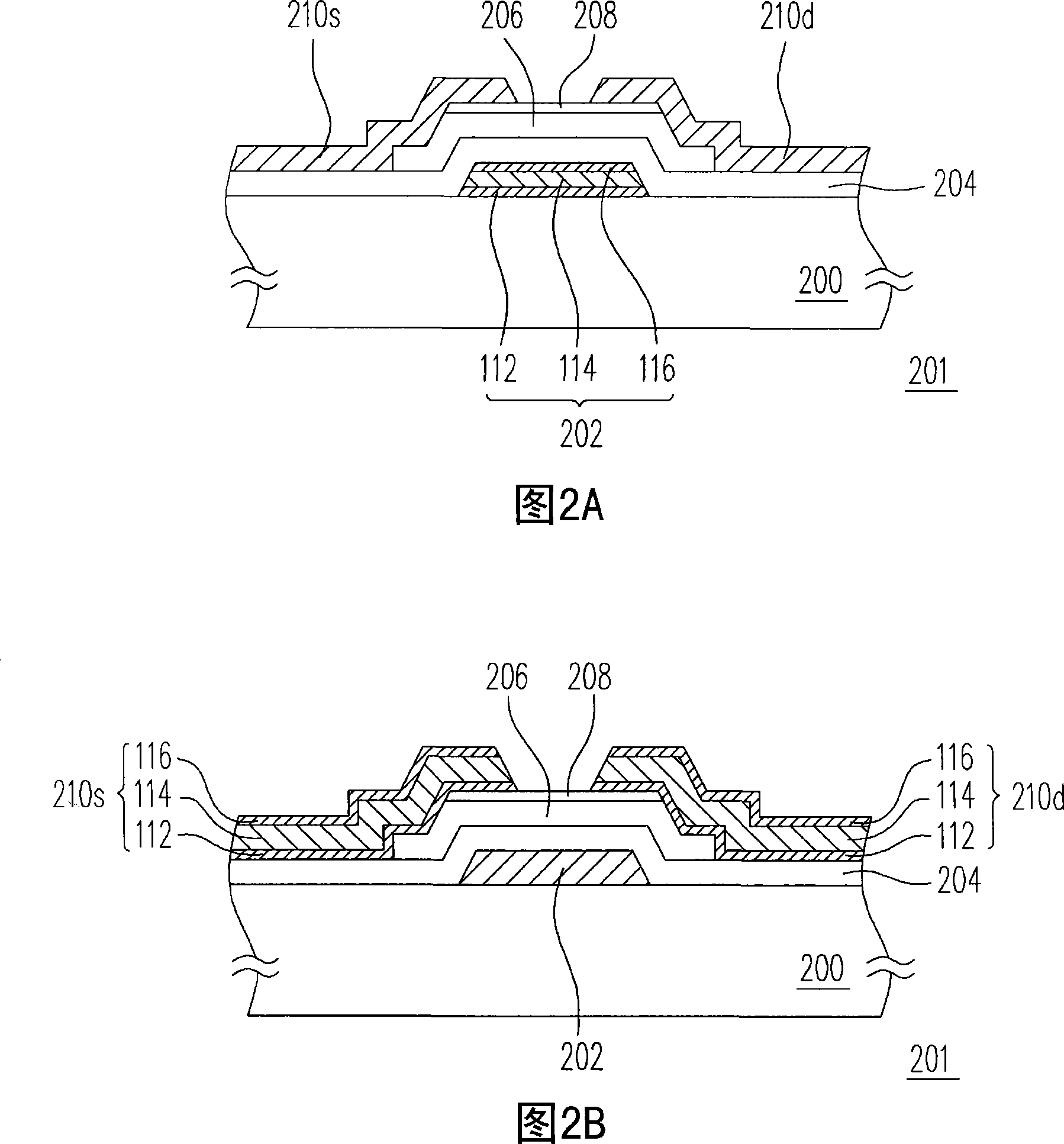
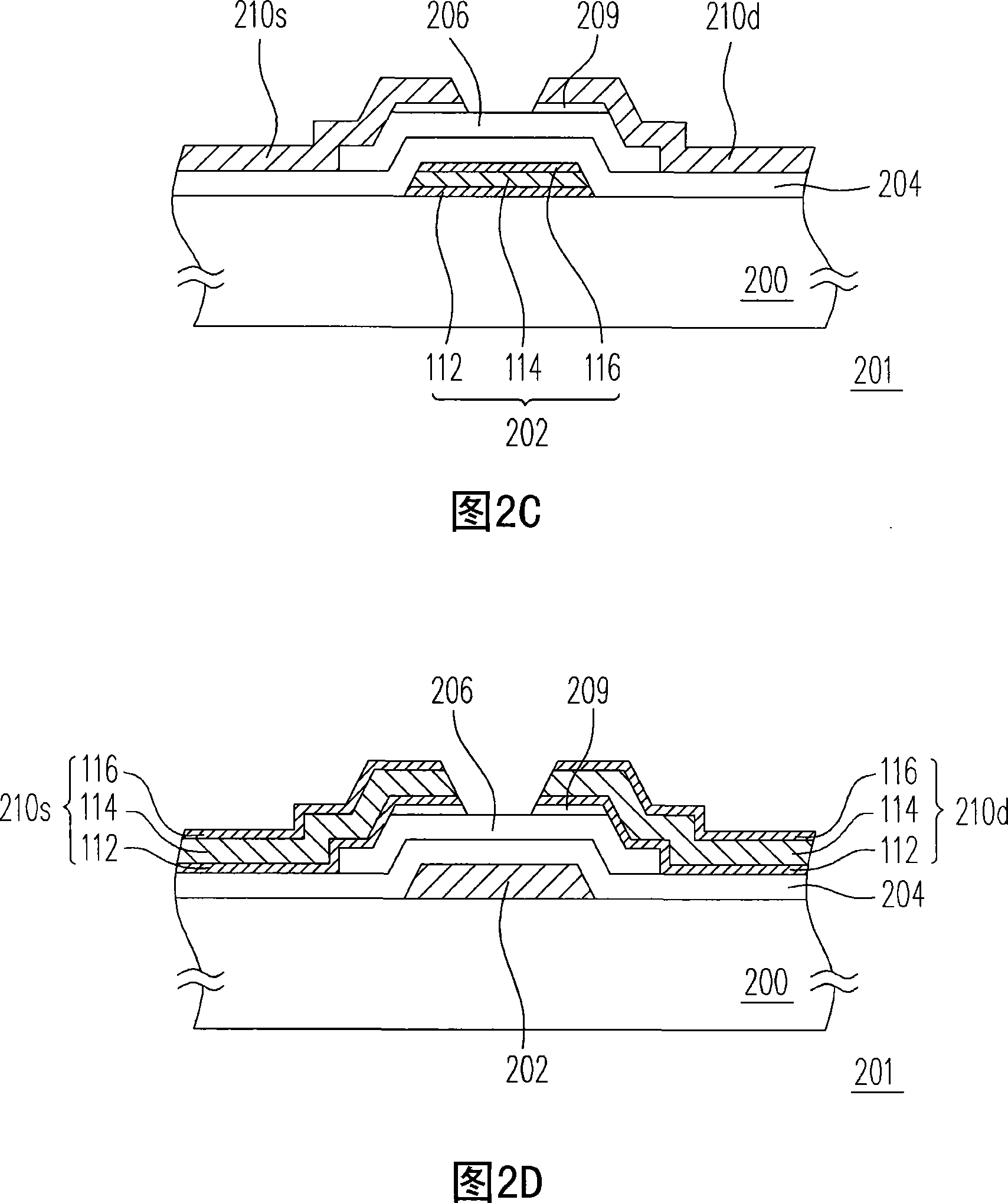
[0070] FIG. 2A is a schematic cross-sectional view of a thin film transistor according to the first embodiment of the present invention. Referring to FIG. 2A , a thin film transistor 201 is disposed on a substrate 200 , which includes a gate 202 , a gate insulating layer 204 , a channel layer 206 , and a source 210s and a drain 210d. Wherein, both the gate 202 and the gate insulating layer 204 are disposed on the substrate 200 , and the gate insulating layer 204 covers the gate 202 . The substrate 200 is, for example, a glass substrate, a quartz substrate or other types of substrates. The material of the gate insulating layer 204 is, for example, silicon oxide, silicon nitride or other dielectric materials. The channel layer 206 is disposed on the gate insulating layer 204 above the gate 202 , wherein the material of the channel layer 206 is, for example, amorphous silicon. The source 210s and the drain 210d are respectively disposed on part of the channel layer 206 on both ...

no. 2 example

[0078] 3A is a schematic top view of an active device array substrate according to a second embodiment of the present invention, and FIGS. 3B and 3C are schematic cross-sectional views along section line a-b and section line c-d in FIG. 3A . Please refer to FIG. 3A , FIG. 3B and FIG. 3C at the same time. In this embodiment, only two pixels 220 in the active device array substrate 20 are shown as a representative for illustration. The active element array substrate 20 includes a substrate 200 , a plurality of scan lines 230 , a plurality of data lines 240 and a plurality of pixels 220 . Scanning lines 230, data lines 240, and pixels 220 are all configured on the substrate 200, wherein a plurality of pixels 220 are respectively connected to corresponding scanning lines 230 and data lines 240, and each pixel 220 includes an active element 216 and an active element 216. The element 216 is electrically connected to the pixel electrode 218 . In addition, in this embodiment, the act...

no. 3 example

[0085] FIG. 4 is a schematic top view of a liquid crystal display panel according to a third embodiment of the present invention. Please refer to FIG. 4, the liquid crystal display panel 10 includes the active element array 20, the opposite substrate 30 and the liquid crystal layer 40 in the above-mentioned embodiment, wherein the opposite substrate 30 is arranged on the opposite side of the active element array substrate 20, and The liquid crystal layer 40 is disposed between the opposite substrate 30 and the active element array substrate 20 . In this embodiment, the opposite substrate 30 is, for example, a color filter substrate, and the liquid crystal display panel 10 may be a transmissive display panel, a semi-transmissive display panel, a reflective display panel, or a color filter on an array. (color filter on array) display panel, array on a color filter (array on color filter) display panel, or other types of substrates.

[0086] Due to the plurality of active elemen...


PUM

PropertyMeasurementUnit
thicknessaaaaaaaaaa
thicknessaaaaaaaaaa
thicknessaaaaaaaaaa

Abstract

The invention discloses a thin film transistor, an active element array base plate and a liquid crystal display panel, wherein the thin film transistor comprises a base plate, a gate, a gate insulating layer, a channel layer, a source electrode and a drain electrode, the gate and the gate insulating layer are arranged on the base plate, and the gate insulating layer is covered on the gate. The channel layer is arranged on the gate insulating layer which is arranged on the upper of the gate, and the source electrode and the drain electrode are respectively arranged on a part of the channel layer, which are arranged on the two sides of the gate. At least one of the gate, the source electrode and the drain electrode is equipped with a conductive interlayer which is equipped with a bottom conductive layer and a top conductive layer and is located between the bottom conductive layer and the top conductive layer, the materials of the bottom conductive layer and the top conductive layer are different, and substantially, the thickness of the bottom conductive layer is smaller or equal to 150 angstrom. An electrode with the above structure is capable of avoiding that the gate, the source electrode and the drain electrode produce an undercut phenomenon during processing, thereby corresponding thin film transistors are capable of normally operating to maintain the element characteristics and the normal operation of a pixel and further maintain the display quality of the corresponding liquid crystal display panel.

Description

technical field [0001] The present invention relates to a structure of a semiconductor element, and in particular to a structure of a thin film transistor. Background technique [0002] In semiconductor manufacturing processes, thin film transistors (Thin Film Transistor, TFT) are often used as switching elements. Generally speaking, a thin film transistor includes a gate, a gate insulating layer, a channel layer, and a source and a drain. Wherein, the gate electrode, the source electrode and the drain electrode are respectively, for example, a single metal layer or a metal stack composed of aluminum, chromium, tungsten, tantalum, titanium and the like. Among the above-mentioned conductive materials, aluminum is widely used in thin film transistors due to its cheap price and many characteristics, such as low resistivity, good adhesion to the substrate, and good etching characteristics. In the electrode structure of the TFT, the electrode of the thin film transistor is, for...

Claims


Application Information

Patent Timeline
Patent Type & Authority Applications(China)
IPC IPC(8): H01L29/786H01L29/40H01L29/41H01L29/417H01L29/423H01L29/43H01L29/49H01L27/12G02F1/1362G02F1/136
Inventor 陈柏林谢婷林俊男蔡文庆
Owner AU OPTRONICS CORP
Why Eureka
Try Eureka