Shallow groove isolation layer of semiconductor element and manufacturing method thereof
A semiconductor and trench technology, used in semiconductor/solid-state device manufacturing, semiconductor devices, electrical components, etc., to achieve the effects of low high temperature shrinkage amplitude, low surface selectivity, and good hole filling ability
- Summary
- Abstract
- Description
- Claims
- Application Information
AI Technical Summary
Problems solved by technology
Method used
Image

Examples
Embodiment Construction
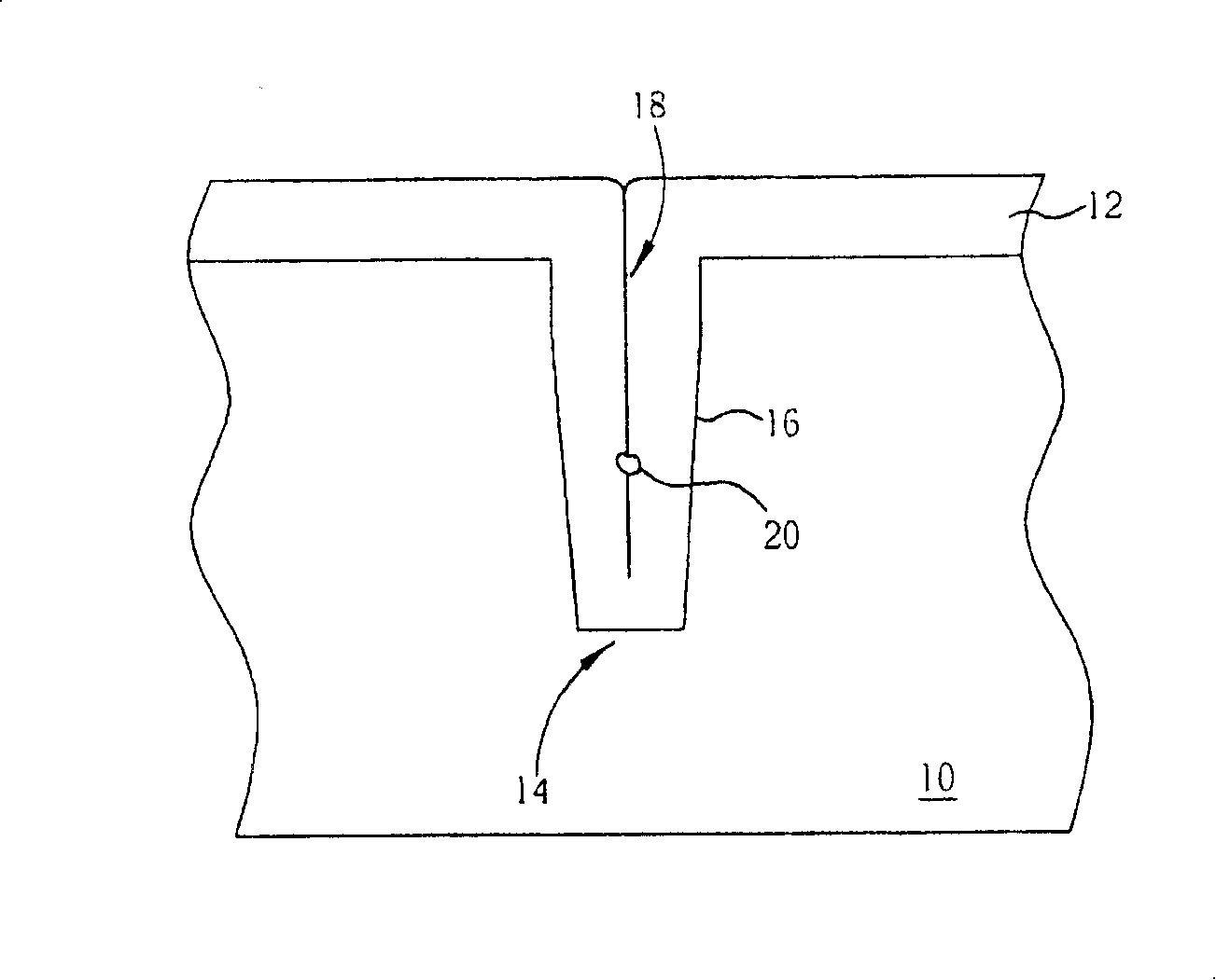
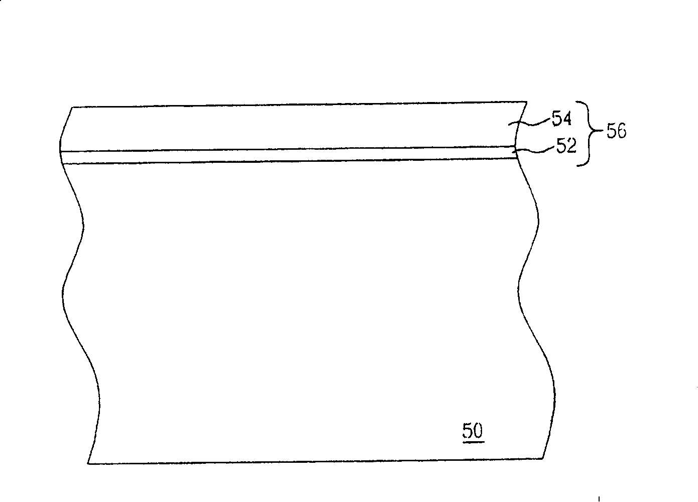
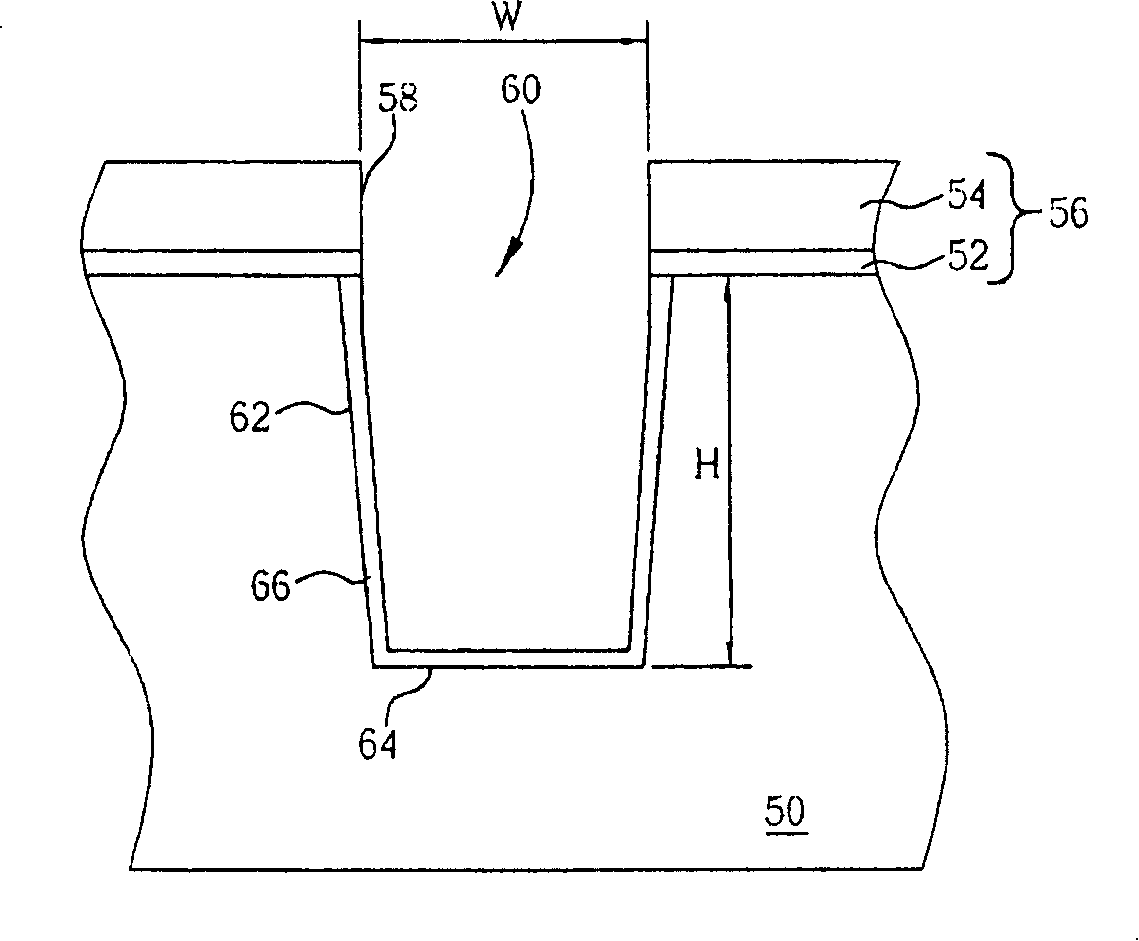
[0038] Please refer to the Figure 2 to Figure 6 , Figure 2 to Figure 6 It is a schematic cross-sectional view of the first embodiment of the shallow trench isolation layer structure and manufacturing process of the present invention. First, if figure 2 As shown, a semiconductor substrate 50, such as a silicon substrate, is provided. Next, a pad oxide layer 52 with a thickness of approximately 30 angstroms to 200 angstroms is formed on the semiconductor substrate 50 . The pad oxide layer 52 can be formed by chemical vapor deposition or thermal oxidation growth. Subsequently, a pad nitride layer 54 with a thickness of approximately 500 angstroms to 2000 angstroms is covered on the pad oxide layer 52 , and together with the pad oxide layer 52 as a shielding layer 56 .
[0039] Then if image 3As shown, an opening 58 is formed in the masking layer 56 by a photolithography process and an etching process, and then the exposed semiconductor substrate 50 is etched downward thr...
PUM
 Abstract
Description
Claims
Application Information
 - R&D
- Intellectual Property
- Life Sciences
- Materials
- Tech Scout
- Unparalleled Data Quality
- Higher Quality Content
- 60% Fewer Hallucinations
Browse by: Latest US Patents, China's latest patents, Technical Efficacy Thesaurus, Application Domain, Technology Topic, Popular Technical Reports.
© 2025 PatSnap. All rights reserved.Legal|Privacy policy|Modern Slavery Act Transparency Statement|Sitemap|About US| Contact US: help@patsnap.com