
Thin membrane crystal cover packaging construction for preventing thin membrane dent forming glue filling bubble

A film-on-chip packaging and glue filling technology, which is applied to electrical components, electrical solid-state devices, circuits, etc., can solve problems such as the inability to fill the gap, the collapse of the circuit film 110, the expansion of the bonding area, and the generation of air bubbles.

Inactive Publication Date: 2008-07-30
CHIPMOS TECH INC
View PDF0 Cites 7 Cited by
  • Summary
  • Abstract
  • Description
  • Claims
  • Application Information

AI Technical Summary

Problems solved by technology

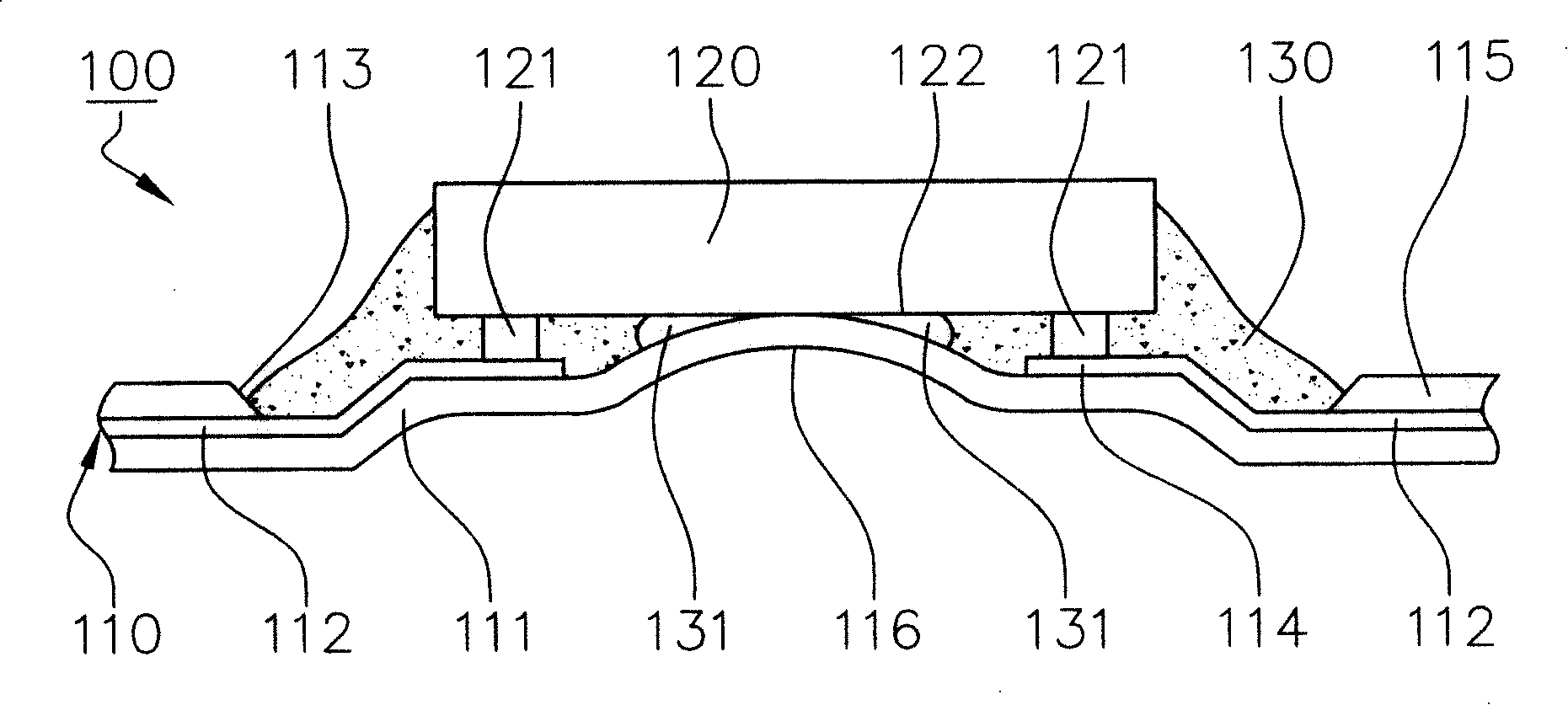
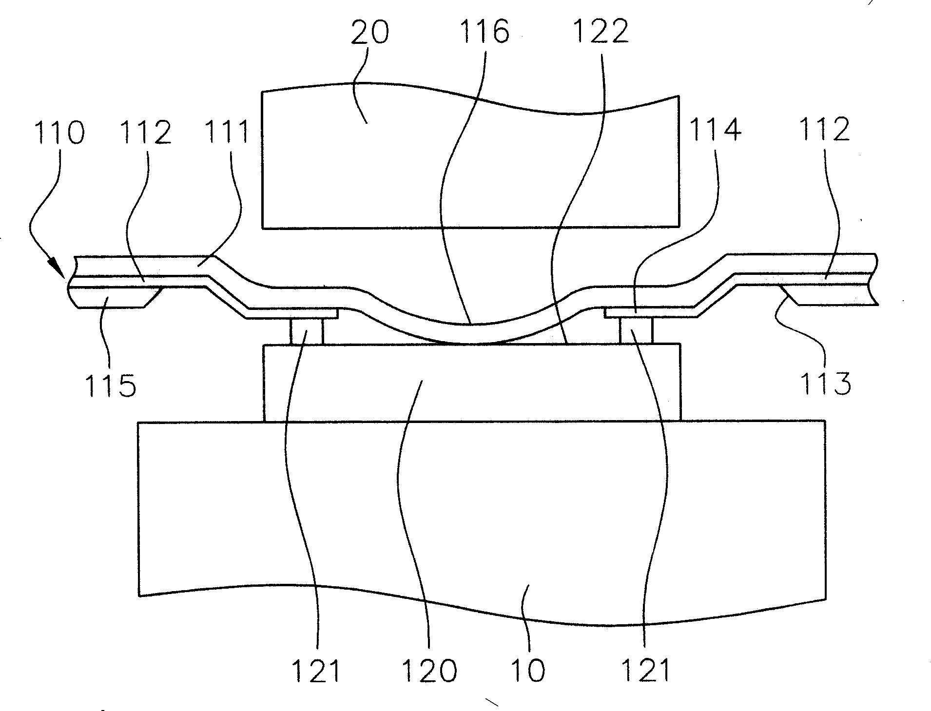
like figure 2 As shown, in the chip bonding process of internal pin bonding, the chip 120 is picked up and placed on a heatable stage 10, and a unit of the circuit film 110 is moved to a fixed position by tape and reel transport, and The high-temperature pressing head 20 of the internal pin bonding equipment presses the circuit film 110 to join the inner ends 114 of the pins 112 and the bumps 121. The circuit film 110 will be heated and cause irreversible collapse and deformation 116. Once The circuit film 110 is directly attached to the active surface 122 of the chip 120, and the high temperature heating from the chip 120 will cause the circuit film 110 to collapse and stick to an expanded and irregular area.
Therefore, in the follow-up dispensing operation, the dispensing glue 130 cannot fill the gap between the wafer 120 and the circuit film 110, and bubbles 131 will be generated at the collapsed deformation 116.

Method used


Image

  • Thin membrane crystal cover packaging construction for preventing thin membrane dent forming glue filling bubble
  • Thin membrane crystal cover packaging construction for preventing thin membrane dent forming glue filling bubble
  • Thin membrane crystal cover packaging construction for preventing thin membrane dent forming glue filling bubble

Examples


no. 1 Embodiment

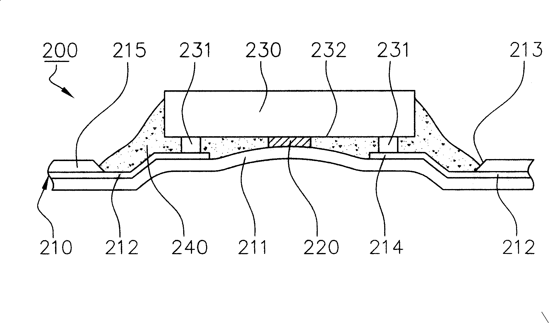
[0058] According to the first embodiment of the present invention, a thin film on chip package structure is disclosed that prevents the thin film from collapsing to form a filling bubble. Such as image 3 As shown, the chip-on-film package structure 200 mainly includes a circuit film 210, a plurality of non-conductor spacers 220, a chip 230, and a dot glue 240. In this embodiment, the non-conductor spacers 220 are first arranged on the circuit film 210 (e.g. Figure 5 Shown).

[0059] Such as image 3 and Figure 4 As shown, the circuit film 210 mainly has a soft dielectric layer 211 and a plurality of pins 212. A wafer bonding area 213 is defined on a surface of the circuit film 210 as a coverage area for bonding the wafer 230. The circuit film 210 may further include a solder resist layer 215 formed on the soft dielectric layer 211 to cover a part of the pins 212. In this embodiment, the chip bonding area 213 is defined by the opening of the solder mask 215.

[0060] Generally, ...


PUM


Abstract

The invention relates to a chip-on-film package configuration for preventing the thin film from forming adhesive bubbles due to recess, which mainly comprises a circuit film, a plurality of non-conductor spacer blocks, a bumped chip and a dispensing adhesive. A plurality of chip bumps are a plurality of inner pins bonded in a chip bonding region defined by the circuit film. The non-conductor spacer blocks can be arranged in the chip bonding region of the circuit film or between bumps on the chip. During chip bonding, the recess caused by the circuit film does not directly contact the chip, the non-conductor spacer blocks thereby provide an adhesive gap and the dispensing adhesive flows to fill the gap between the circuit film and the chip, thus preventing the thin film from forming bubbles.

Description

Technical field [0001] The present invention relates to a chip-on-film package (COF package), in particular to a chip-on-film package (COF package), which prevents the film from collapsing to form glue-filled bubbles. Background technique [0002] Among the many types of integrated circuit packaging, the chip-on-film packaging (COF) uses bumped chips to bond a circuit film and seal it appropriately. At present, there are many techniques for bonding the bumps of the chip and the inner pins on the film, such as Eutectic bonding, NCP bonding, and ACF bonding. )and many more. Based on the consideration of cost reduction and equipment continued use, inner lead bonding can be used in thin film flip chip packaging, and the inner lead bonding equipment of tape-and-reel package (TCP) can be used. During the chip bonding, the pressing head of the inner pin bonding directly pressurizes and heats the circuit film, which often causes the circuit film to be heated to produce permanent deformat...

Claims


Application Information

Patent Timeline
Patent Type & Authority Applications(China)
IPC IPC(8): H01L23/498H01L23/31
CPCH01L2224/73204
Inventor 陈纬铭李明勋梁锦坤
Owner CHIPMOS TECH INC
Learn More