
Method for manufacturing printed circuit board with built-in capacitor

A technology of printed wiring board and manufacturing method, which is applied in the direction of printed circuit manufacturing, capacitors, fixed capacitors, etc., can solve the problems of difficulty in component manufacturing and installation, the need for component cost and installation cost, and the inability to make small capacitance capacitors and large capacitance capacitors, etc., to achieve The effect of preventing short circuit

Inactive Publication Date: 2008-07-30
NIPPON MEKTRON LTD
View PDF4 Cites 3 Cited by
  • Summary
  • Abstract
  • Description
  • Claims
  • Application Information

AI Technical Summary

Problems solved by technology

[0008] As the problem of the prior art, the following problems can be cited: it is difficult to manufacture and mount parts for miniaturization of the size below the above, and in addition, about 250 capacitors are mounted in each mobile phone, so parts are required cost and installation cost
Moreover, in the prior art, it is not possible to manufacture small-capacitance capacitors and large-capacitance capacitors with high precision by the same method.

Method used


Image

  • Method for manufacturing printed circuit board with built-in capacitor
  • Method for manufacturing printed circuit board with built-in capacitor

Examples


Embodiment Construction

[0038] Hereinafter, the present invention will be further described with reference to the illustrated embodiments.

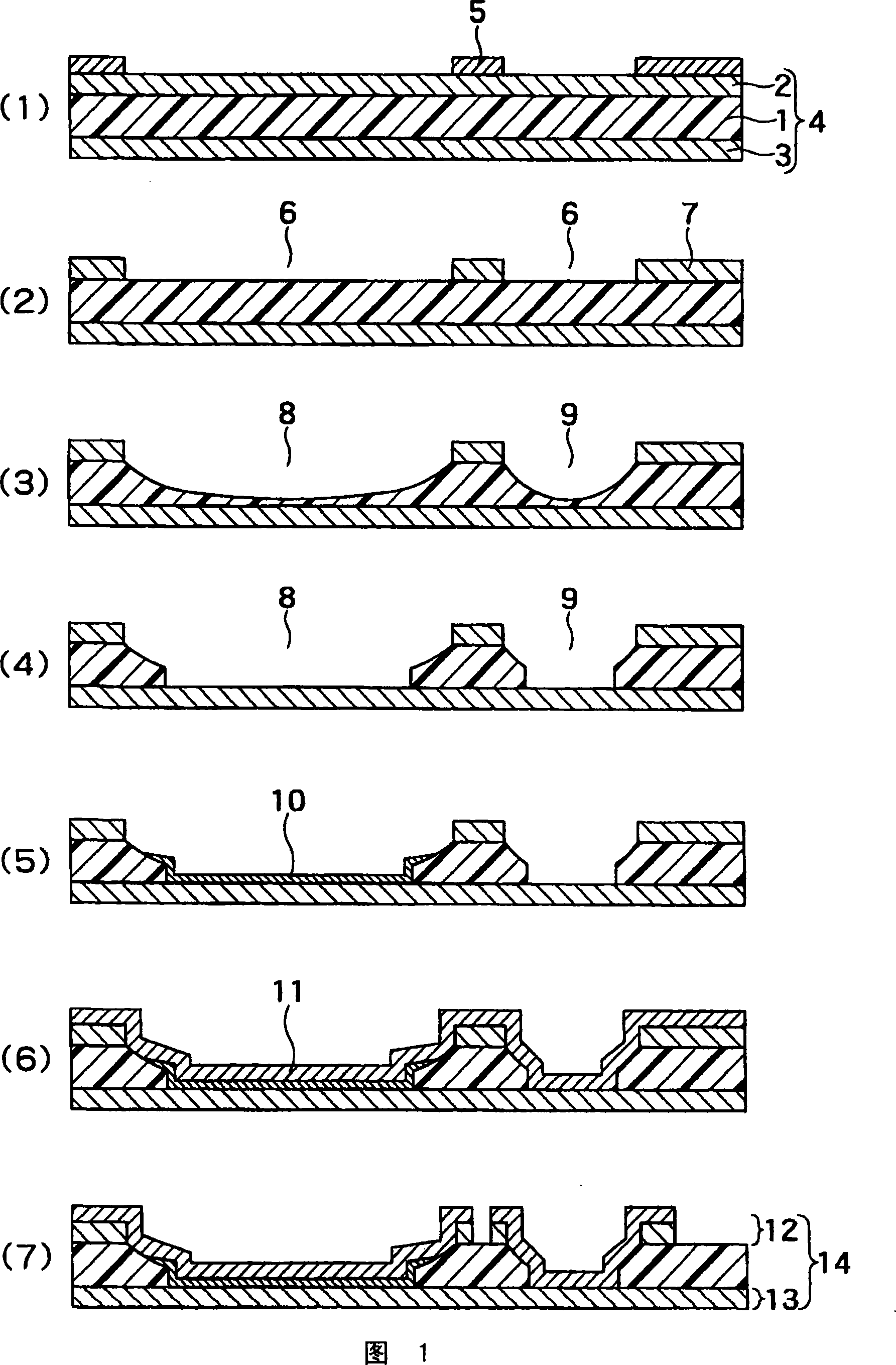
[0039] FIG. 1 is a cross-sectional view showing a method of manufacturing a printed wiring board incorporating a capacitor structure according to an embodiment of the present invention. In this method, first, as shown in FIG. 1(1), a so-called flexible insulating base material 1 having a first metal foil 2 such as copper foil and a second metal foil 3 on both sides of a flexible insulating base material 1 such as polyimide is prepared. For the double-sided copper-clad laminate 4, a resist layer 5 is formed on the desired position of the first metal foil 2 by using an etching method using a usual photochemical etching manufacturing method. The portion where the hole is formed has a metal mask with an opening.

[0040] In this step, it is preferable to stick a dry film resist or the like using a laminator or the like. Also, 25 μm thick polyimide was used as the ...


PUM


Abstract

A method for producing a printing wiring plate with an internal capacitor of a high-frequency midget capacitor, a decoupling capacitor and an EMI filter capacitor with high accuracy by a same method, characterized in that: preparing an insulated substrate material (1) having a first and second metal foils (2), (3) on each surface respectively; setting an opening of a metal mask (7) on said first metal foil; using the metal mask, removing said insulated substrate material exposing from the opening of the metal mask in the manner of continuous inclined plane from periphery of the metal mask towards the central part; removing the insulated substrate material with the inclined plane with the diameter less than the metal mask to expose the second metal foil; forming a dielectric medium layer (10) by a print method according to the following manner, e.g., covering the second metal foil exposing from the insulated substrate material by an area less than the metal mask but more than the second metal foil exposing from the insulated substrate material; forming a conductive layer on the dielectric medium layer as a first electrode, and taking the surface of the second metal foil contacting the dielectric medium layer as a second electrode.

Description

technical field [0001] The invention relates to a structure and a manufacturing method of a printed wiring board, in particular to a manufacturing method of a printed wiring board with a built-in capacitor structure. Background technique [0002] In recent years, printed wiring boards have been required to be lighter in weight, and in order to mount small, multi-pin BGA (Ball Grid Array) or PGA (Pin Grid Array), CSP (Chip Scale Package), etc., wiring miniaturization and high densification. [0003] However, as wiring becomes denser, each wiring pattern is close to each other, causing problems such as crosstalk noise between wirings, potential fluctuations in power lines, ground lines, and the like. [0004] In particular, when semiconductor elements or electronic components that require high-speed switching operations are mounted, crosstalk noise is likely to be generated along with an increase in frequency, and switching noise is generated due to high-speed ON / OFF of switc...

Claims


Application Information

Patent Timeline
Patent Type & Authority Applications(China)
IPC IPC(8): H05K3/00H05K1/16H01G4/00
CPCH01G4/252H01G4/01H05K3/0041H05K3/002H05K2201/09509H05K2201/0355H05K2201/0394H05K3/0035H05K1/162
Inventor 宫本雅郎
Owner NIPPON MEKTRON LTD
Learn More