Nano crystal silicon and non crystal germanium mixed absorption layer for multi-node light voltage part based on film silicon

A nanocrystalline silicon and photovoltaic device technology, applied in photovoltaic power generation, semiconductor devices, electrical components, etc., can solve the problem of low open circuit voltage, poor stability, and high defect density of amorphous silicon germanium solar cells. question

Inactive Publication Date: 2008-08-06
BEIJING XINGZHE MULTIMEDIA TECH
View PDF2 Cites 12 Cited by
  • Summary
  • Abstract
  • Description
  • Claims
  • Application Information

AI Technical Summary

Problems solved by technology

When used alone as the i-layer material, the high defect density and poor stability of amorphous silicon germanium make it unable to compare with

Method used


Image

  • Nano crystal silicon and non crystal germanium mixed absorption layer for multi-node light voltage part based on film silicon
  • Nano crystal silicon and non crystal germanium mixed absorption layer for multi-node light voltage part based on film silicon
  • Nano crystal silicon and non crystal germanium mixed absorption layer for multi-node light voltage part based on film silicon

Examples


Embodiment 1

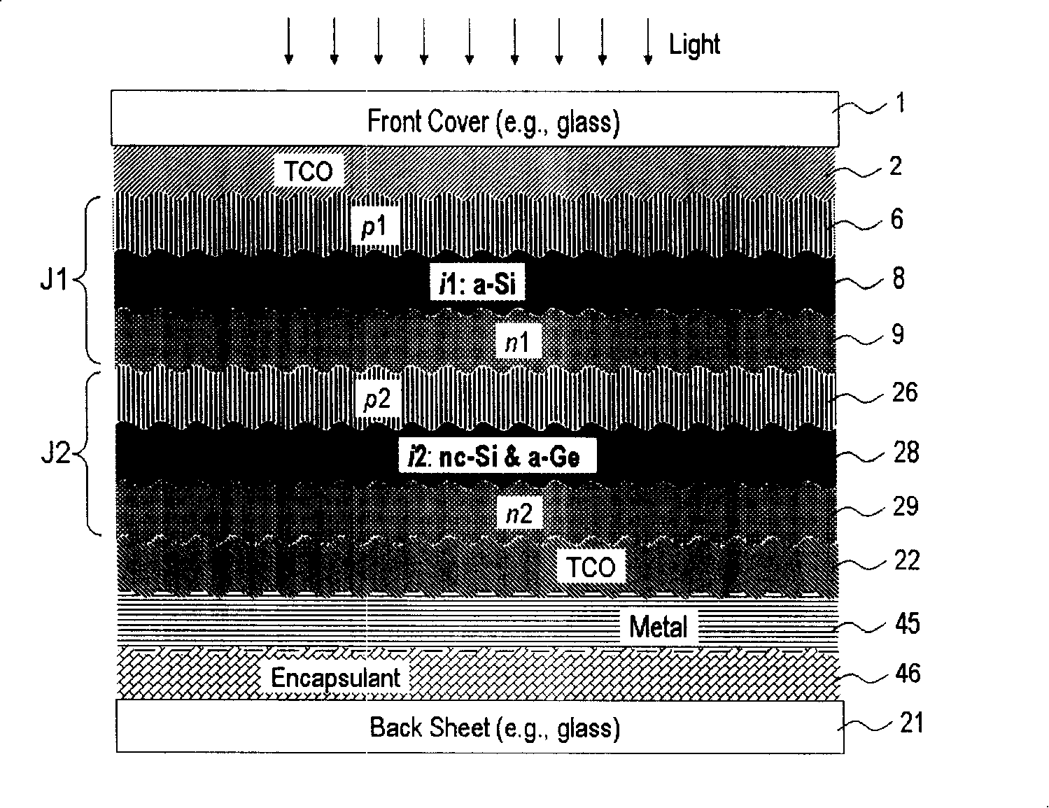
[0038] Figure 2 relates to a double-junction thin-film silicon-based photovoltaic device. The device comprises two junction photovoltaic cells, a junction top cell 6-8-9 (p1-i1-n1) and a junction bottom cell 26-28-29 (p2-i2-n2). The double-junction photovoltaic cell is placed on a transparent electrode 2 supported by a substrate 1 . Transparent electrodes are generally made of fluorine-doped tin oxide (SnO 2 ) such a transparent conductive oxide (TCO) film. The rough (textured) surface of tin oxide is suitable for scattering light, thus enhancing the light absorption capacity of the photovoltaic layer. The transparent conductive oxide film layer 22 and the metal film layer 45 together form the light reflective electrode on the back of the photovoltaic device. This device is encapsulated in film layer 46 and protective film 21 . The p1 layer 6 material of the top cell is usually a boron-doped wide-bandgap amorphous silicon alloy, such as amorphous silicon carbon, amorphous ...

Embodiment 2

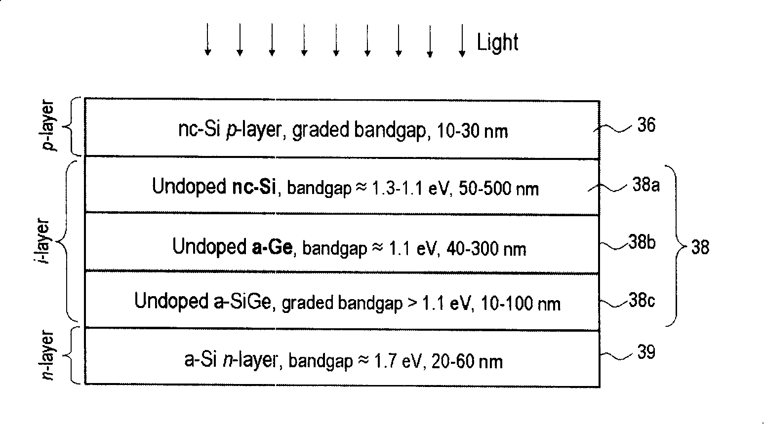
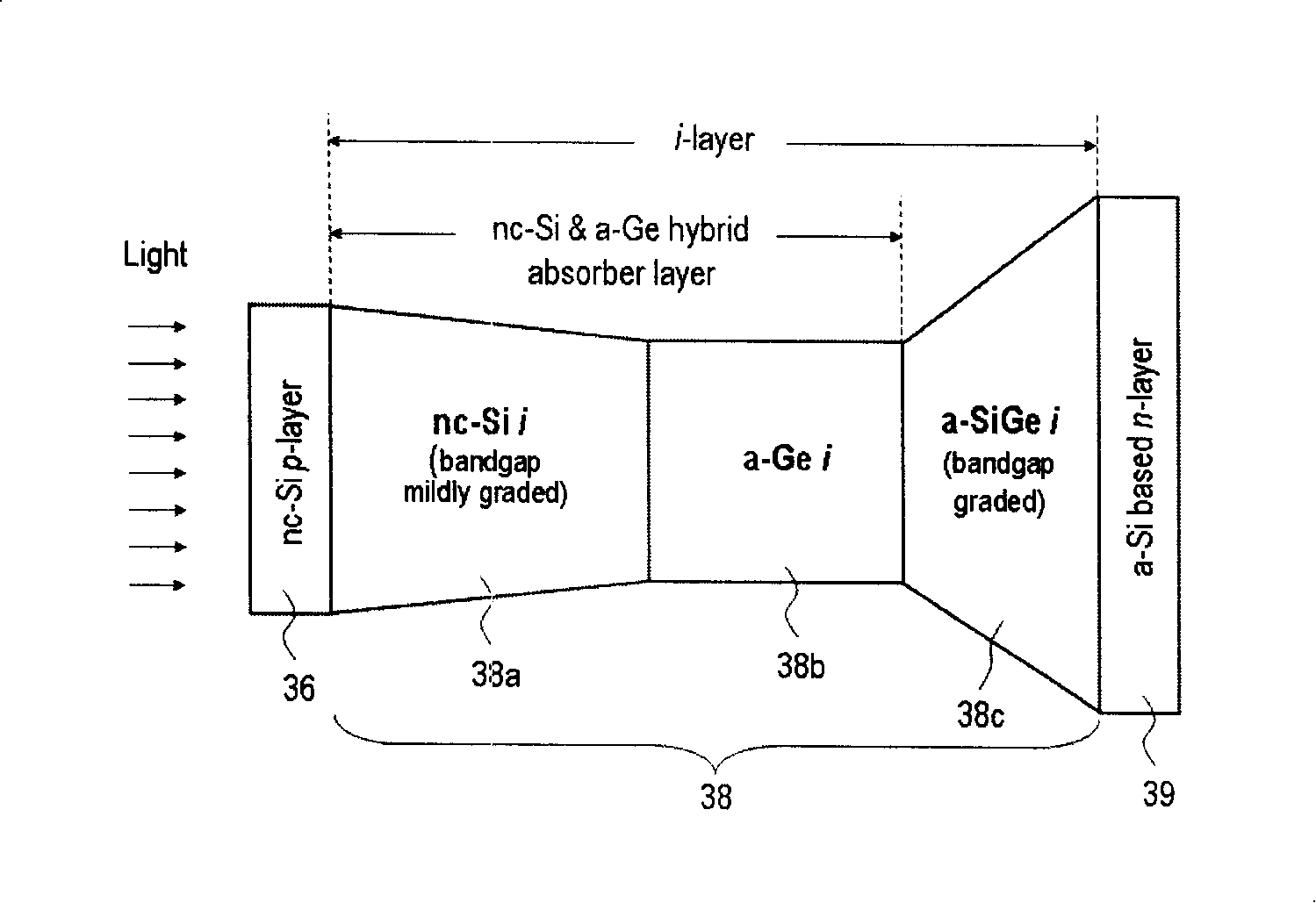
[0042] A triple-junction photovoltaic device based on thin-film silicon consists of three stacked p-i-n photovoltaic cells with the same optical path and the same electrical path. The bandgaps of the i-layers in each junction photovoltaic cell can be the same but preferably are different. Such as image 3 As shown, a triple-junction thin-film silicon-based photovoltaic device includes three p-i-n cells J1, J2 and J3 arranged together. The front electrode 2 is deposited on the substrate 1, the light-reflecting electrodes 22 and 45, the encapsulant 46 and the back protection sheet 21 are the same as in the double junction photovoltaic device shown in FIG. 2 . The top, middle and bottom cells contain p1-i1-n1(6-8-9), p2-i2-n2(26-28-29), and p3-i3-n3(36-38-39), respectively. The absorber or intrinsic layers i1, i2(8,28) of the top and middle cells are preferably made of amorphous silicon and amorphous silicon germanium, or amorphous silicon and nanocrystalline silicon (amorphous...


PUM

PropertyMeasurementUnit
Thicknessaaaaaaaaaa
Thicknessaaaaaaaaaa
Bandgapaaaaaaaaaa

Abstract

The present invention discloses a p-i-n type photovoltaic battery which comprises a novel i layer absorption layer with a narrow band gap. The front part of the absorption layer is made from nanometer crystal silicon, the middle part is made from amorphous germanium material, and the back part is made from amorphous germanium silicon. The photovoltaic battery comprising a mixed-type i layer can be perfectly utilized as a base layer battery of a multi-junction photovoltaic device based on the silicon film. The photovoltaic battery has the advantages of good performance, strong reliability and low production cost.

Description

technical field [0001] The invention relates to a p-i-n type thin-film silicon photovoltaic device, which contains a semiconductor photoelectric conversion layer with narrow band gap inside. The invention particularly relates to a mixed type narrow-bandgap intrinsic i-layer, the intrinsic i-layer includes nano-crystalline silicon and amorphous germanium, and they form a continuous laminated structure in the i-layer through a plasma chemical vapor deposition method. Background technique [0002] In recent years, thin-film photovoltaic cells and large-area photovoltaic modules have attracted worldwide attention. Hydrogenated amorphous silicon and nanocrystalline silicon, in particular, have shown great potential with the widespread adoption of photovoltaic devices in commercial and residential installations. A notable feature of producing thin-film silicon photovoltaic devices at a relatively low temperature below 260°C is that semiconductor films and electrical contact films...

Claims


Application Information

Patent Timeline
IPC IPC(8): H01L31/075H01L31/042H01L31/20H01L31/0352H01L31/076
CPCY02E10/50Y02E10/548Y02P70/50
Inventor 李沅民马昕
Owner BEIJING XINGZHE MULTIMEDIA TECH
Why Eureka
Try Eureka