Realization method for 3-D integrated circuit based on SOI round slice

A technology of integrated circuits and implementation methods, which is applied in the manufacture of circuits, electrical components, semiconductors/solid-state devices, etc., can solve problems affecting bonding quality, damage to integrated circuits, and increased costs, and achieve high density, avoid flattening requirements, The effect of occupying a small area

Active Publication Date: 2008-08-13
TSINGHUA UNIV
View PDF0 Cites 26 Cited by
  • Summary
  • Abstract
  • Description
  • Claims
  • Application Information

AI Technical Summary

Problems solved by technology

However, due to the very high requirements for the flatness of the surfaces of the two bonded wafers, which generally reach the atomic level, that is, sub-nanometer level, strict surface planarization treatment must be carried out before bonding, which becomes a manufacturing difficulty and increases In addition, direct bonding of silicon dioxide has high requirements on annealing temperature. Usually, annealing below 600°C is difficult to meet the requirements of direct bonding of silicon diox...

Method used


Image

  • Realization method for 3-D integrated circuit based on SOI round slice
  • Realization method for 3-D integrated circuit based on SOI round slice
  • Realization method for 3-D integrated circuit based on SOI round slice

Examples


Embodiment Construction

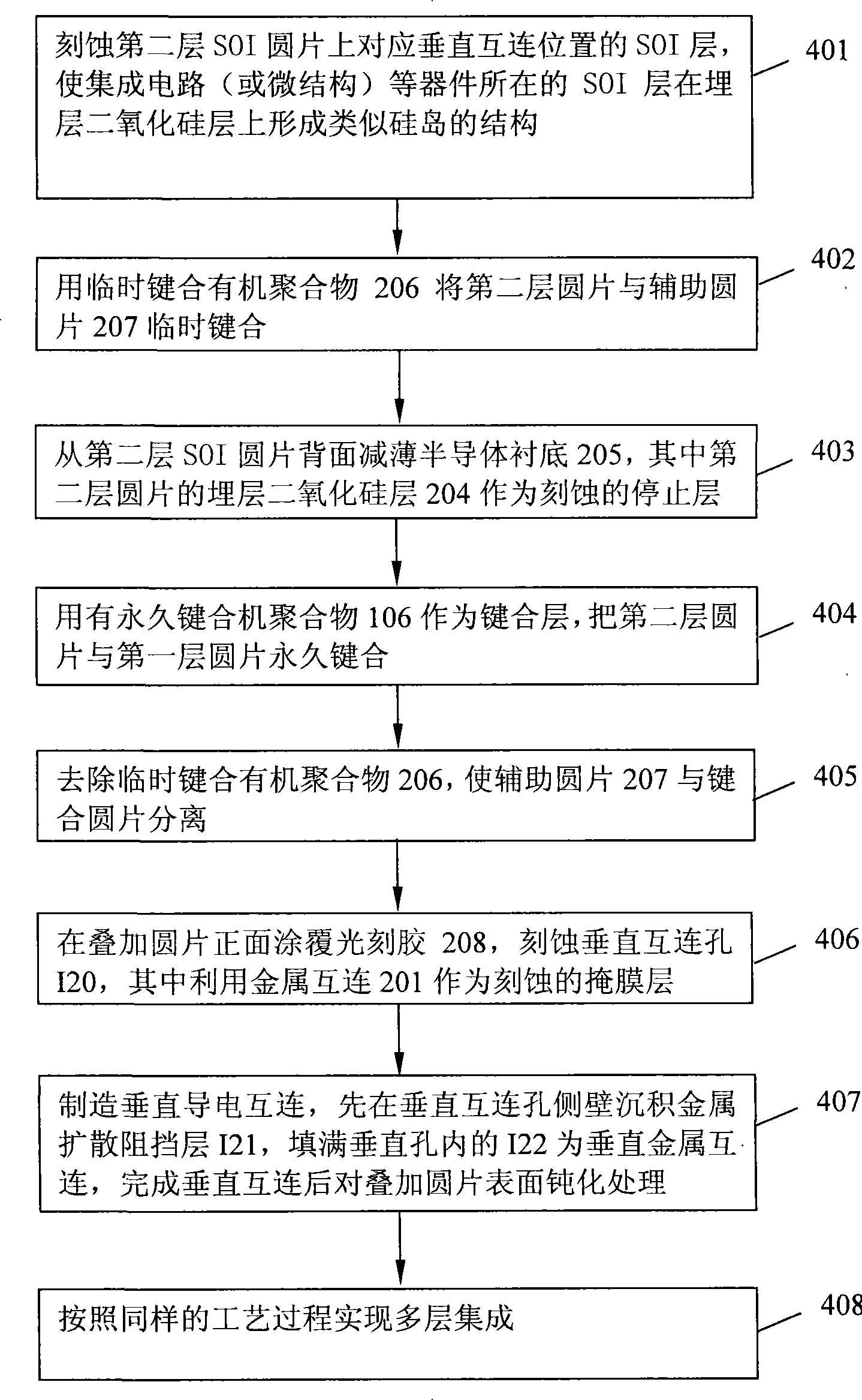
[0036] In order to make the object, technical solution and advantages of the present invention clearer, the implementation manner of the present invention will be further described in detail below in conjunction with the accompanying drawings. An embodiment of the present invention provides a method for realizing a three-dimensional integrated circuit based on an SOI wafer, which can effectively realize a single-layer very thin and very compact three-dimensional integrated circuit.

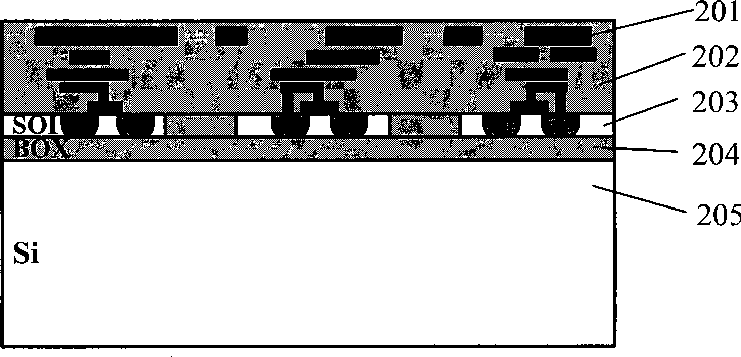
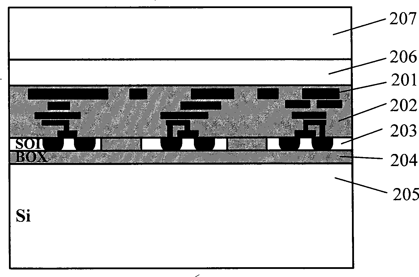
[0037] see figure 1 , this embodiment provides a manufacturing process of a method for realizing a three-dimensional integrated circuit based on an SOI wafer. see figure 2 , as shown in the figure, the second semiconductor wafer is an SOI wafer, including a semiconductor substrate (Si) 205, a buried silicon dioxide layer (BOX layer) 204, a silicon-on-insulator layer (SOI layer) 203, and a surface passivation layer. layer 202 and metal interconnection 201. Integrated circuits (or microstructure...


PUM


Abstract

The invention discloses an implementation method of three-dimensional integrated circuit based on SOI disk. The method includes: etching removing the SOI device layer which perpendicularly interconnects with the silicon (SOI) disk on the insulator manufacturing the integrated circuit; utilizing the organic polymer to temporarily bond the SOI disk on the supplementary disk so as to remove the displacing the SOI layer to the supplementary disk by the SOI disk substrate; utilizing the organic polymer to implement the back to front permanent bonding of temporary displacing the SOI disk with another bottom disk manufacturing the integrated circuit so as to form the stack disks; front etching the silicon dioxide layer and the permanent bonding layer form the stack disks and filling metal for implementing the perpendicular interconnection of the SOI layer disk with the bottom disk. The invention manufactures the perpendicular interconnection on the insulating position so as to solve the problem that the lateral wall of the deep hole is insulating, and reduces the manufacturing degree of difficulty of the three-dimensional integration. The method can be used in integrated circuit and micro sensor field for implementing three-dimensional integration of the back to front bonding of the multilayer chip.

Description

technical field [0001] The invention belongs to the field of semiconductor manufacturing technology, three-dimensional integration technology, and sensor manufacturing technology, and particularly relates to a method for realizing a three-dimensional integrated circuit based on an SOI wafer. Background technique [0002] The continuous reduction of integrated circuit feature size and the continuous improvement of integration not only make the feature size of integrated circuits gradually approach the physical limit, but also make integrated circuits encounter insurmountable development bottlenecks in terms of design, manufacturing and cost. At present, the feature size of complementary metal-oxide-semiconductor (CMOS) integrated circuits has entered 65nm, and the speed of the device itself is continuously increasing, and 1 billion CMOS devices can be integrated on a chip area per square centimeter. This makes the total length of metal interconnect lines on high-end integrate...

Claims


Application Information

Patent Timeline
IPC IPC(8): H01L21/84H01L21/768
Inventor 王喆垚陈倩文宋崇申蔡坚刘理天
Owner TSINGHUA UNIV
Why Eureka
Try Eureka