Method and circuit of driving electron-emitting device, electron source, and image-forming apparatus

一种电子发射装置、电子发射的技术,应用在电路、放电管电子枪、放电管主电极等方向,能够解决降低图象对比度等问题,达到抑制电子发射、高性能的效果

Inactive Publication Date: 2008-08-20
CANON KK
View PDF2 Cites 0 Cited by
  • Summary
  • Abstract
  • Description
  • Claims
  • Application Information

AI Technical Summary

Problems solved by technology

[0034] If an imaging device is constructed using a device that emits electrons even in the OFF phase, pixels that should be in the OFF state (dark state) during the OFF phase will be in the ON state (light-emitting state), thereby reducing the generation of the device. image contrast

Method used


Image

  • Method and circuit of driving electron-emitting device, electron source, and image-forming apparatus
  • Method and circuit of driving electron-emitting device, electron source, and image-forming apparatus
  • Method and circuit of driving electron-emitting device, electron source, and image-forming apparatus

Examples


no. 1 example

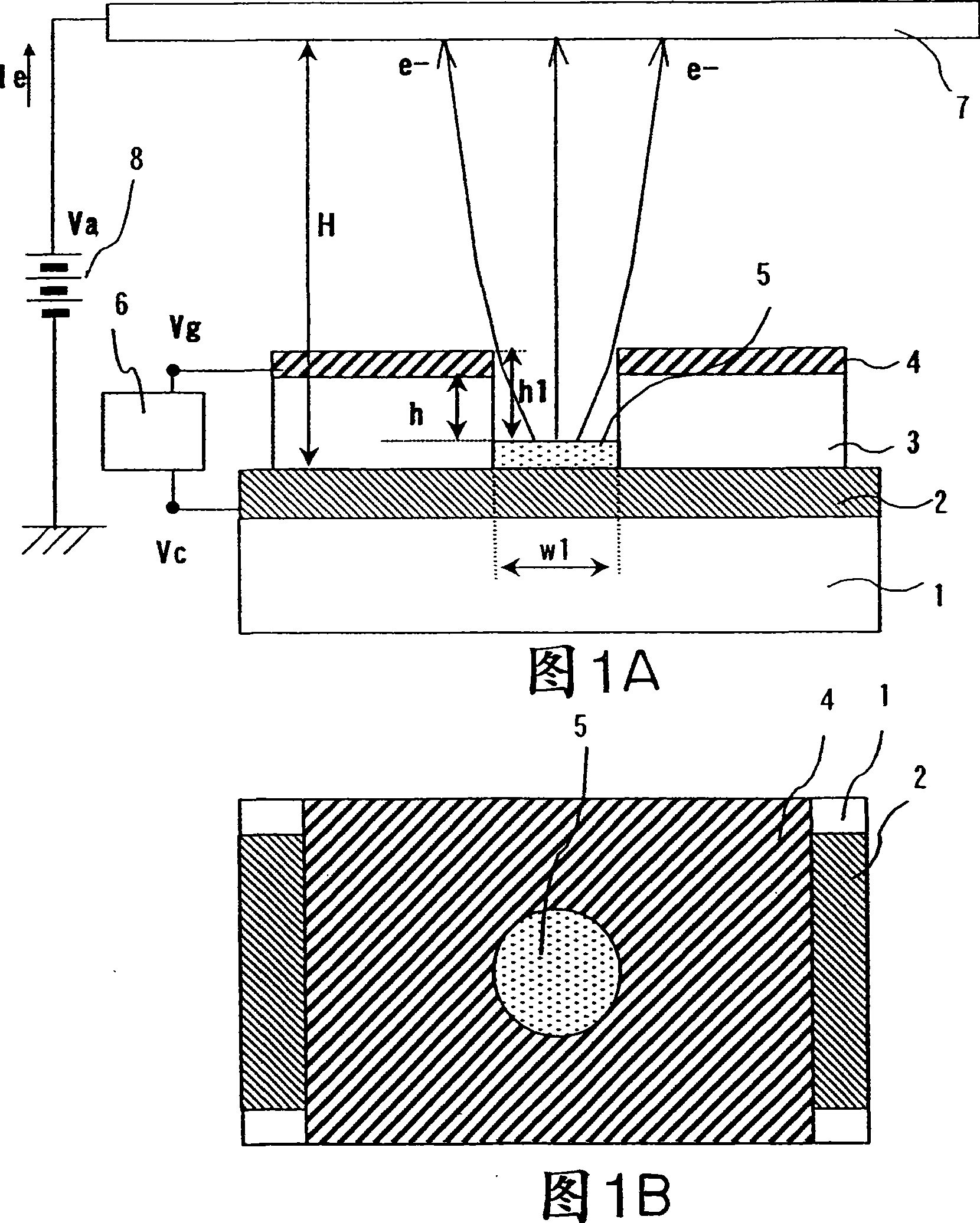
[0224] 1A and 1B are a plan view and a cross-sectional view of the electron-emitting device of the first embodiment, and FIG. 6 shows a method of manufacturing the device. A method of manufacturing the electron emission device of this example is described in detail below.

[0225] (step 1)

[0226] First, as shown in FIG. 6A, a substrate 1 is prepared by sufficiently cleaning quartz glass. Next, a Ta thin film with a thickness of 300 nm was formed as the cathode electrode 2 by a sputtering method.

[0227] (step 2)

[0228] Next, as shown in FIG. 6B, an insulating layer 3 and a gate electrode 4 are stacked in sequence, wherein the insulating layer 3 is SiO with a thickness of 600 nm. 2 thin film, the gate electrode 4 is a Ta thin film with a thickness of 100 nm.

[0229] (step 3)

[0230] Then, as shown in FIG. 6C, a photomask pattern of a positive photoresist (AZ1500 manufactured by Clariant) was formed by spin coating, exposed to light, and developed using photolithogra...

no. 2 example

[0244]Another control method of the present invention is described in this embodiment.

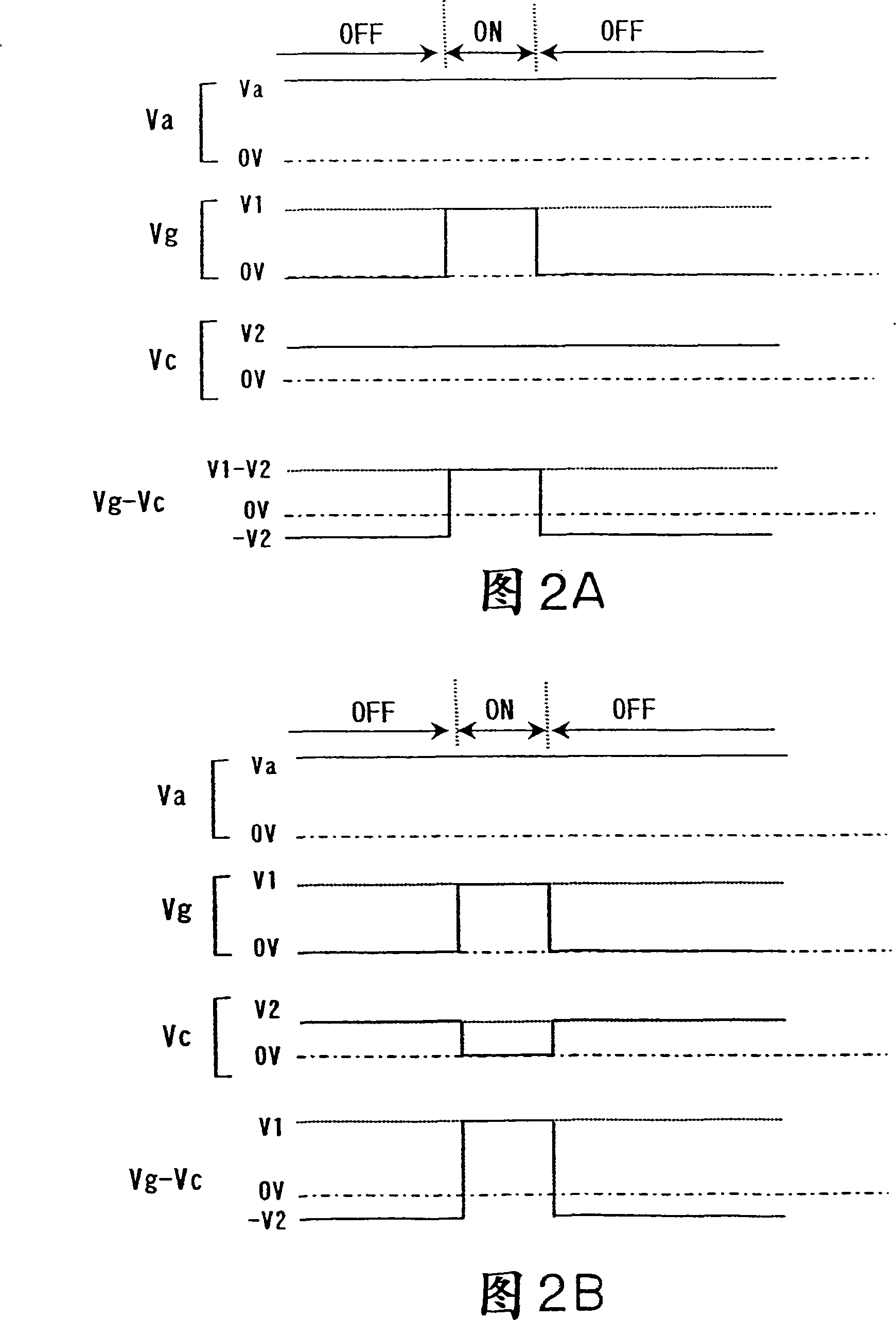
[0245] As in the first embodiment, the electron-emitting device shown in FIG. 1 is also used in this embodiment. However, the distance H between the device and the anode electrode 7 was set to 1 mm, and the anode electrode voltage Va was set to 15 KV in this embodiment.

[0246] The control operation shown in FIG. 2B is performed in this embodiment. In addition, as the second comparative example, the voltages V1 and V2 can be set to 15V and 0V, respectively, like the first comparative example described in the first embodiment.

[0247] With this structure of this example, the electric field strength between the device and the anode electrode 7 is three times that of the first embodiment.

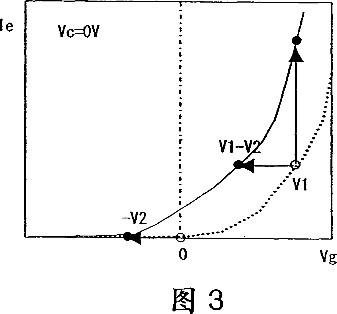
[0248] If the voltage V2 is set to 2V as in the first embodiment, the electron emission current Ie remains in the OFF period. Therefore, the voltage V2 is set to 4V. On the other hand, even if the vo...

no. 3 example

[0254] In this embodiment, the image forming apparatus shown in FIG. 9 is constructed using an electron source including a plurality of electron emission devices of the second embodiment, which are wired in a matrix as shown in FIG. 7 . In addition, the driving circuit shown in FIG. 11 is formed in the device and the control operation shown in FIG. 12 is executed. The voltages Vx1, Vx2, and Vy1 are set to 4V, 20V, and 16V, respectively. In addition, like the second embodiment, as a third comparative example, the voltages V1 and V2 are set to 16V and 0V, respectively, and the voltages Vg and Vc in the OFF stage are both set to 0V. In order to compare Control devices with passive matrix configuration.

[0255] The electron-emitting devices may be arranged such that both the X-direction interval and the Y-direction interval are set to 150 μm. A fluorescent film 74 is provided on the device. In the third comparative example, the contrast was lowered due to this structure, and a...


PUM


Abstract

Disclosed are methods for driving an electron-emitting device, an electron source, and an image-forming apparatus, driving circuits for an electron source and an image-forming apparatus, and an electron source and an image-forming apparatus, with each of which electron emission is effectively halted. A voltage (Vg-Vc)>0 is applied to an electron-emitting device placed in a driving state in which electrons should be emitted, thereby having the electron-emitting device emit electrons. A voltage (Vg-Vc)<0 is applied to an electron-emitting device placed in a halt state in which no electrons should be emitted, thereby having the electron-emitting device halt electron emission. In this manner, an electric field that is formed between a cathode electrode and a gate electrode in the halt state becomes opposite to an electric field that is formed therebetween in the driving state, thereby easily weakening an electric field directed toward an anode electrode and effectively suppressing electron emission in the halt state.

Description

[0001] This application is a divisional application with a filing date of September 21, 2001, an application number of 01145682.5, and an invention title of "Method and Circuit for Driving Electron Emission Devices, Electron Sources and Imaging Devices". technical field [0002] The present invention relates to a method of driving an electron emission device, an electron source and an imaging device. Background technique [0003] Conventionally, two types of electron-emitting devices have been known, which are a hot cathode electron emission source and a cold cathode electron emission source. The cold cathode electron emission sources include electric field emission type (hereinafter referred to as FE type) devices, metal / insulator / metal type devices (hereinafter referred to as MIM type) and surface conduction electron emission devices. [0004] By W.P.Dyke and W.W.Dolan in "Field Emission", Advance in Electronics and Physics, 8, 89 (1956) and C.A. Spindt in "Physical Proper...

Claims


Application Information

Patent Timeline
Patent Type & Authority Applications(China)
IPC IPC(8): G09G3/22H01J3/02H04N5/70H01J9/02G09G3/20H01J1/30H01J1/304H01J29/04H01J31/12
CPCH01J3/022G09G3/22G09G2320/02G09G2320/0238H04N5/70H01J1/30
Inventor 西村三千代笹栗大助野村和司
Owner CANON KK
Why Eureka
Try Eureka