Method for reinforcing optical capturing effect of thin film photovoltaic device

A photovoltaic device and thin-film silicon technology, applied in the field of solar photovoltaic equipment, can solve the problem that the reflected light cannot reach the critical angle, etc.

Inactive Publication Date: 2008-08-20
BEIJING XINGZHE MULTIMEDIA TECH
View PDF0 Cites 6 Cited by
  • Summary
  • Abstract
  • Description
  • Claims
  • Application Information

AI Technical Summary

Problems solved by technology

However, since the reflective back electrode has a relatively flat interface with the n-layer, the angle of reflected light usually does not reach the critical angle for total internal reflection.

Method used


Image

  • Method for reinforcing optical capturing effect of thin film photovoltaic device

Examples


Embodiment Construction

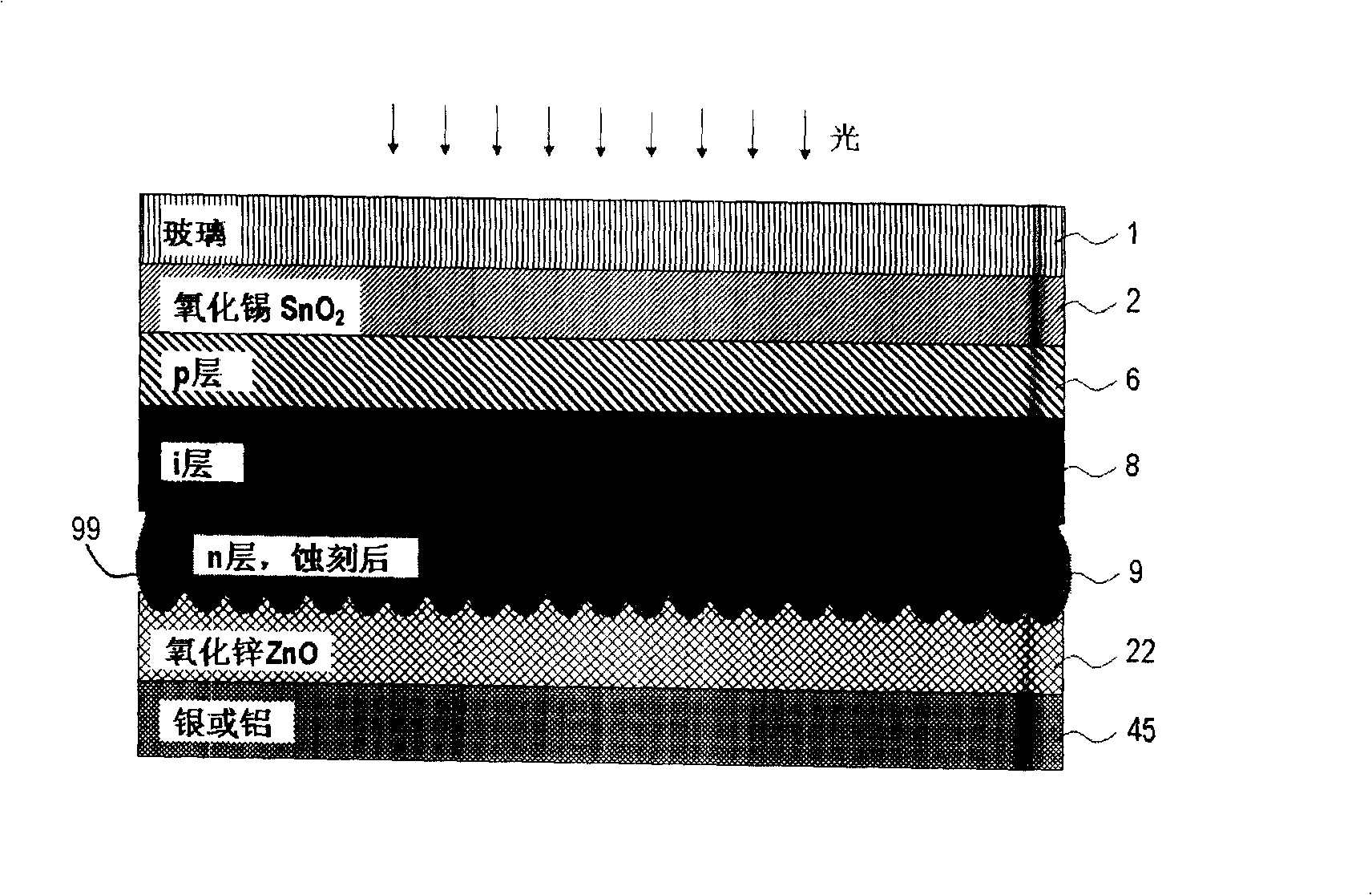
[0011] As shown in the accompanying drawing, a p-i-n type photovoltaic device comprises: a glass substrate 1; a transparent conductive front contact layer 2, a boron-doped p-layer 6 based on thin-film silicon, an intrinsic thin-film silicon-based i-layer 8 , a phosphorus-doped n-layer 9 based on thin-film silicon and a highly reflective back electrode composed of metal oxide 22 and metal film 45 . When the p-i-n layer is obtained by plasma-enhanced chemical vapor deposition, the present invention intentionally makes the n-layer relatively thick, such as not less than 300 nanometers. After this, the device is treated with an etch plasma, using plasma source gases including hydrogen, fluorine-containing gases, and chlorine-containing gases, such as NF 3 , CCl 4 . This plasma etching process is carried out under relatively high pressure, such as greater than 4mbar, and at relatively high power, so that the etching process has obvious regional and non-uniformity. As a result, t...


PUM


Abstract

The present invention discloses a method for inducing long wave radiation of improved film silicon p-i-n type solar cell which is characterized of etching process a thicker n layer to make it has a non-flat structure with micron dimension, and the high reflection back electrode on the back makes the long wave light not be absorbed entering photovoltaic conversion layer again with bigger angle. So the whole inner reflection effect is gained, and the capture of weak absorption light is improved, and the conversion efficiency of silicon film solar photovoltaic device is improved.

Description

technical field [0001] The invention belongs to the field of solar photovoltaic devices, in particular to the manufacturing technology of thin-film silicon-based photovoltaic devices. Background technique [0002] In recent years, the development of photovoltaic cells and large-area photovoltaic modules has attracted widespread attention in the world. Hydrogenated amorphous silicon and nanocrystalline silicon, in particular, have shown great potential with the widespread adoption of photovoltaic devices in commercial and residential installations. A notable feature of producing thin-film silicon photovoltaic devices at such a low temperature below 260°C is that the large-area deposited silicon-related semiconductor film layers and electrical contact film layers have excellent performance. At the same time, using well-established coating equipment and procedures, low-cost stencils can be produced industrially. Laser patterning of different thin films applied on the same gla...

Claims


Application Information

Patent Timeline
Patent Type & Authority Applications(China)
IPC IPC(8): H01L31/075H01L31/042H01L31/02H01L31/0224H01L31/0236
CPCY02E10/548
Inventor 李沅民马昕
Owner BEIJING XINGZHE MULTIMEDIA TECH
Why Eureka
Try Eureka