Defect correction method and manufacturing method for grey level mask and grey level mask

A grayscale mask and defect technology, which is applied to the photolithographic process of pattern surface, the original used for photomechanical processing, and the exposure device of photolithographic process, can solve the problem of small light transmission and improve the controllability , stable and proper correction, high precision effect

Inactive Publication Date: 2012-09-26
HOYA CORP +1
View PDF4 Cites 0 Cited by
  • Summary
  • Abstract
  • Description
  • Claims
  • Application Information

AI Technical Summary

Problems solved by technology

At this time, if a correction film 28c having a uniform film thickness is formed on the defective portion ( Image 6 (b)), then since the correction film is formed on the semi-transmissive film 26 that remains partially in the white defect portion, the problem that the light transmission amount in the area where the semi-transmissive film and the correction film overlap occurs is less than the desired value (refer to Image 6 (c) Sectional view)

Method used


Image

  • Defect correction method and manufacturing method for grey level mask and grey level mask
  • Defect correction method and manufacturing method for grey level mask and grey level mask
  • Defect correction method and manufacturing method for grey level mask and grey level mask

Examples


no. 1 approach

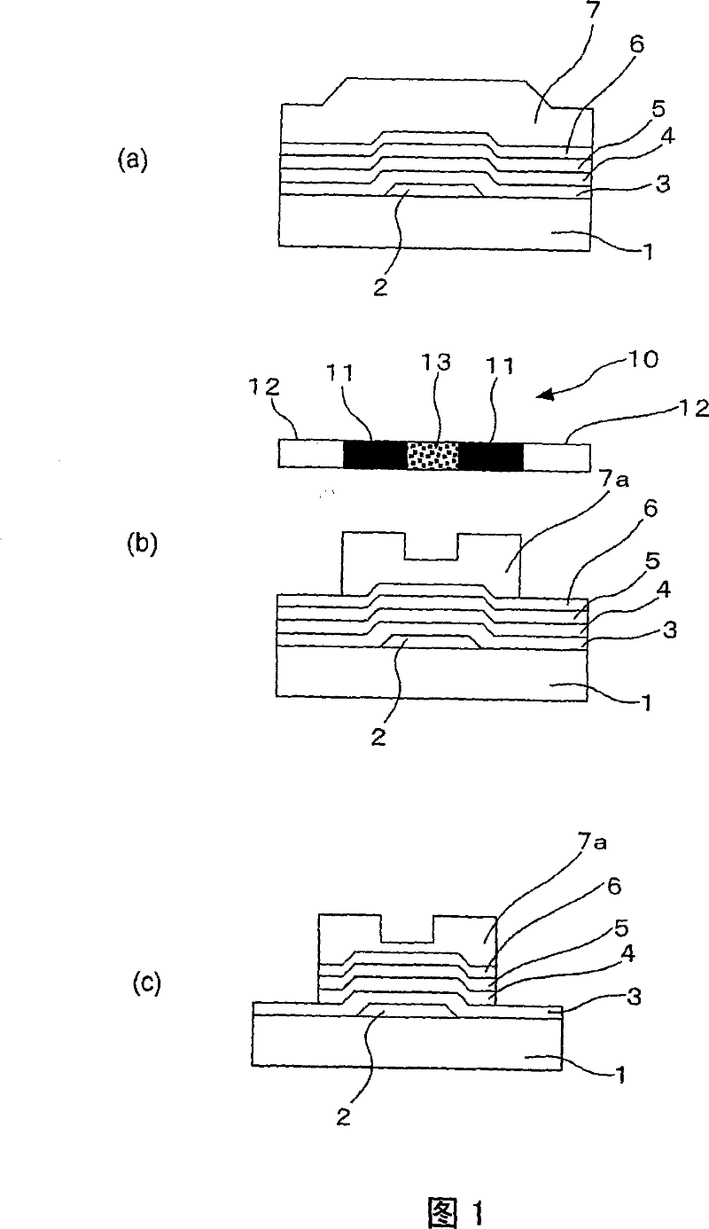
[0059] Figure 8 (a)~ Figure 8 (d) shows the first embodiment of the defect correction method of the gray scale mask related to the present invention, Figure 8 (a)~ Figure 8 (c) are perspective views illustrating a defect correction method in order of steps, respectively, Figure 8 (d) is Figure 8 Side sectional view along line L-L in (c). in addition, Figure 9 It is a sectional view for explaining the pattern transfer method using the gray scale mask of this invention. and, Figure 9 The corrected defective portion is not shown.

[0060] Figure 9 The grayscale mask 20 of the present invention shown is used to manufacture thin film transistors (TFT) or color filters of liquid crystal display devices (LCD), or plasma display panels (PDP), etc., and is formed on the transferred body 30. The resist pattern 33 having a stepwise or continuous film thickness. in addition, Figure 9 Symbols 32A and 32B in , represent films laminated on the substrate 31 in the body to...

no. 2 approach

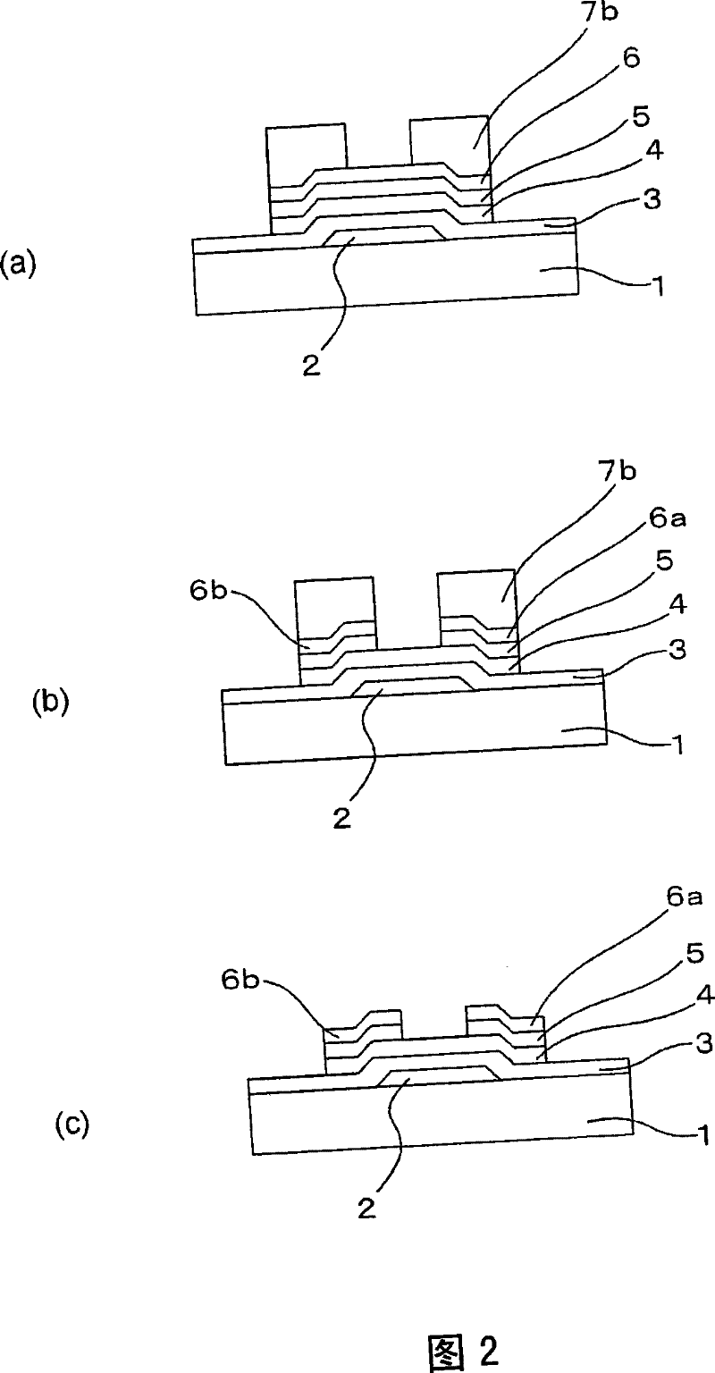
[0086] Figure 11 (a)~ Figure 11 (d) shows the second embodiment of the defect correction method of the grayscale mask related to the present invention, Figure 11 (a)~ Figure 11 (c) is a perspective view illustrating each defect correction method in order of steps, Figure 11 (d) is Figure 11 Side sectional view along line L-L in (c).

[0087] Figure 6 (a)~ Figure 6 As also explained in (c), the actual white defect does not necessarily have a shape in which the cross section is substantially perpendicular to the film thickness direction. For example Figure 11 As shown in (a), sometimes a white defect 52 is formed in the light semi-transmissive film 26, and the defect is shaped like a mortar, and the cross-section gradually becomes narrower toward the transparent substrate 24 side. At this time, if a correction film with a uniform film thickness is formed on the defect site, the correction film is formed on the half-transmissive film 26 which remains partly in th...

no. 3 approach

[0092] Figure 12 (a), Figure 12 (b) shows the third embodiment of the defect correction method of the grayscale mask according to the present invention, and is a perspective view illustrating the defect correction method in order of steps.

[0093] When the size of the white defect generated in the semi-transparent portion of the grayscale mask exceeds a certain area, for example, when the film formation area of ​​the correction film is determined in the same way as in the first embodiment, the area that is an integral multiple of the certain area is defined as Defect correction area.

[0094] First, in the third embodiment, when using a film-forming apparatus and a film-forming material determined in the same manner as in the first embodiment, the film-forming area of ​​the correction film is determined so as to achieve a constant exposure light transmission amount.

[0095] Then, when the size of the white defect generated in the semi-transparent part exceeds the above-m...


PUM


Abstract

The invention provides a grey scale mask. A semi-light-permeable film and a lightproof film are formed on a transparent substrate, a lightproof part and a light-permeable part formed by applying a predetermined pattern, and a semi-light-permeable part with a lowered predetermined amount of the permeable amount of exposed light are used for forming anti-corrosion patterns having different film thick stages and continuities on a transferred body. The semi-light-permeable part is formed by a half-hue film. In the flaw correction method of grey scale masks, when a flaw occurs in the semi-light-permeable part, the flaw part is determined, a filming device and a filming material for forming a correction film on the determined flaw part is determined, the filming area is determined when the determined filming device and the filming material are used, such that the permeable amount of exposed light is within a predetermined scope, thus a correction film of the determined filming area is formed.

Description

technical field [0001] The present invention relates to a defect correction method of a gray tone mask used in the manufacture of a liquid crystal display (Liquid Crystal Display: hereinafter referred to as LCD), etc., a method of manufacturing a gray tone mask, and a gray tone mask. The invention relates to a defect correction method of a grayscale mask suitable for use in the manufacture of a thin film transistor substrate (TFT substrate) for manufacturing a thin film transistor liquid crystal display device, a method of manufacturing the grayscale mask, and the grayscale mask. Background technique [0002] Currently, in the LCD field, thin film transistor liquid crystal display (Thin Film Transistor Liquid Crystal Display: hereinafter referred to as TFT-LCD) has the advantages of thinner and lower power consumption compared with CRT (cathode ray tube), so commercial products was rapidly advanced. TFT-LCD has such a general structure: a TFT substrate with a TFT structure ...

Claims


Application Information

Patent Timeline
Patent Type & Authority Patents(China)
IPC IPC(8): G03F1/32G03F1/74G03F7/20G03F1/72
CPCG03F1/32G03F1/72
Inventor 坂本有司
Owner HOYA CORP
Why Eureka
Try Eureka