Whirl etching system and method for large area silicon chips

A rotary etching and large-area technology, which is applied in chemical instruments and methods, crystal growth, electrical components, etc., can solve problems such as inconsistent corrosion speed, different flatness of silicon wafers, and inability to fully stir, so as to improve production efficiency and control temperature precise effect

Inactive Publication Date: 2008-10-01
ZHUZHOU CSR TIMES ELECTRIC CO LTD
View PDF1 Cites 27 Cited by
  • Summary
  • Abstract
  • Description
  • Claims
  • Application Information

AI Technical Summary

Problems solved by technology

This method improves the temperature and concentration uniformity of the etching solution in the horizontal direction to a certain extent, but the concentration and temperature of the etching solution in the vertical direction have not been effectively mixed uniformly, and the etching speed of multiple silicon wafers

Method used


Image

  • Whirl etching system and method for large area silicon chips
  • Whirl etching system and method for large area silicon chips
  • Whirl etching system and method for large area silicon chips

Examples


Embodiment 1

[0032] Figure 2 to Figure 8 It is a schematic diagram of Embodiment 1 of the spin etching system for large-area silicon wafers.

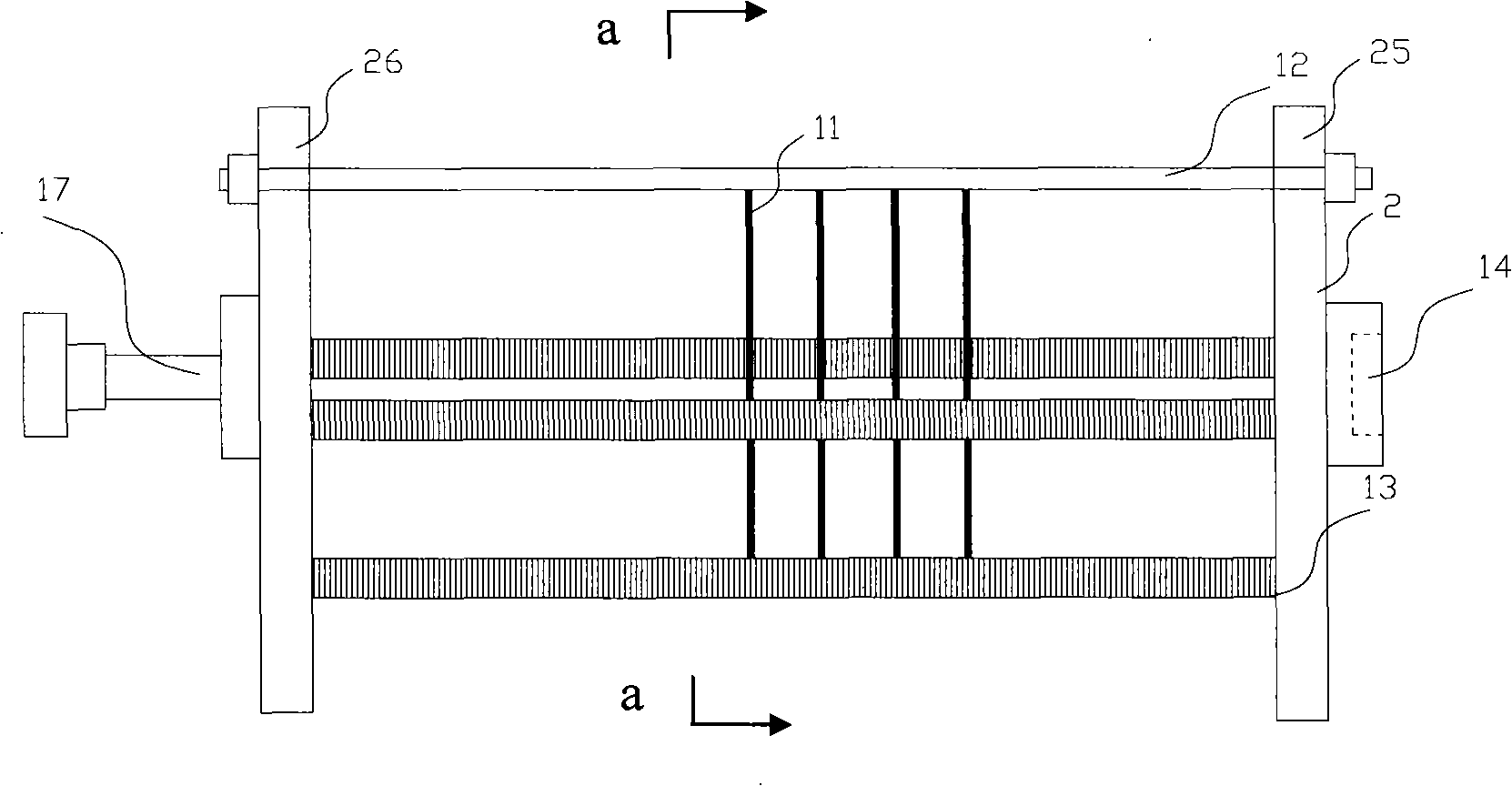
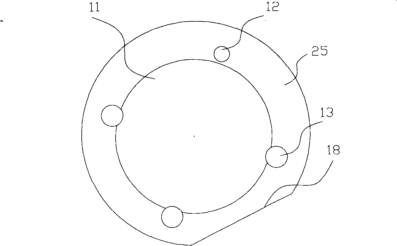
[0033] Silicon wafers with measured and recorded thicknesses were mounted on Figure 2 ~ Figure 4 shown on the rotating corrosion fixture, where, figure 2 Shown is a schematic front view of the rotating corrosion fixture, image 3 Shown is a schematic left view of the cross-section of the fixture along the a-a direction, Figure 4 Shown is the schematic view of the right side view of the clamp after the support bar 12 is removed. Described clamp 2 is made up of four evenly distributed support rods 12,13 and two circular baffles 25,26 connected thereto, and the purpose of platform 18 on the baffle is to facilitate the placement of the clamp, wherein three fixed support rods 13 There are grooves engraved on it to fix the silicon chip. The diameter of the detachable support rod 12 is smaller than that of the other three. When loading the silicon ...

Embodiment 2

[0038] Figure 9 ~ Figure 12It is a schematic diagram of the second embodiment of the spin etching system for large-area silicon wafers.

[0039] Silicon wafers with measured and recorded thicknesses are loaded into Figure 9 The rotary corrosion fixture is shown on 2. Described clamp 2 is made up of four evenly distributed support rods 12,13 and two circular baffles 25,26 connected thereto, and the purpose of platform 18 on the baffle is to facilitate the placement of the clamp, wherein three fixed support rods 13 There are grooves engraved on it to fix the silicon chip. The diameter of the detachable support rod 12 is smaller than that of the other three. When loading the silicon chip, remove it from the groove 16 to leave a space, then put the silicon chip 11 into it, and then install it. The upper detachable support rod 12, which is just in contact with the edge of the silicon wafer 11 to play a position-limiting role; the driven gear 29 is connected with the rotating sh...

Embodiment 3

[0043] Figure 13 is a schematic flow chart of the spin etching method for large-area silicon wafers, Figure 14 ~ Figure 18 It is a schematic diagram of an embodiment of a spin etching method for a large-area silicon wafer.

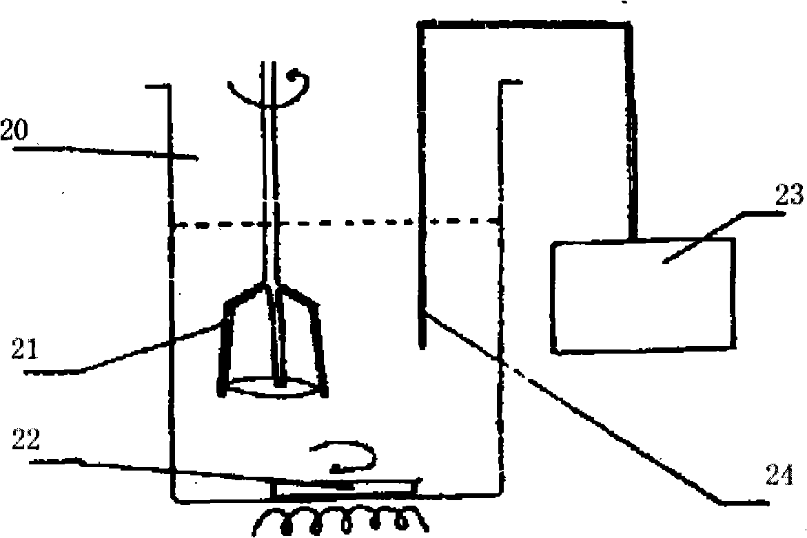
[0044] Step 201: Refer to Figure 14 As shown, the silicon wafer whose thickness has been measured and recorded is rotated on the corrosion fixture 2. The fixture 2 is made up of four evenly distributed support rods 12, 13 and two circular baffles 25, 26 connected thereto. The purpose of the platform 18 is to facilitate the placement of the clamps. Three of the fixed support rods 13 are engraved with grooves to fix the silicon chip. The diameter of the detachable support rod 12 is smaller than the other three. Then remove the silicon chip 11 to leave a space, and then install the detachable support rod 12, which just comes into contact with the edge of the silicon chip 11 to play a position-limiting role.

[0045] Step 202: Refer to Figure 15 As sho...


PUM


Abstract

The invention discloses a whirl etching system for large-area silicon chip and a method thereof, comprising an autorotation etch fixture, a revolution arm, an etch bath, a de-ionized water rinse bath, a bubbling agitating device, a condensing and temperature control device; the etch fixture is installed on the arm for uniform autorotation driven by a rotating motor; the etch bath contains chemical corrosive liquid; the bubbling agitating device is located at bottom of the bath; the condenser pipe and the temperature control thermoelectric couple are installed at side wall of the etch bath; the de-ionized water rinse bath is located adjacent to the etch bath; when etching the silicon chip, the arm drives autorotation fixture into dip into the chemical corrosive liquid in the etch bath, while the arm undergoes uniform revolution; after that, the autorotation fixture driven by the arm is dipped into the de-ionized water rinse bath for cleaning; controlling the temperature of the corrosive liquid, and mixing the corrosive liquid evenly by the agitating device, so as to ensure that the concentration, the temperature of the corrosive liquid is substantially uniform, and that etch speed on the surface of the silicon chip is consistent, so as to enhance uniformity of silicon chip etching.

Description

technical field [0001] The invention relates to the technical field of semiconductor manufacturing, in particular to a large-area silicon wafer spin etching system and method. Background technique [0002] With the continuous improvement of thyristor manufacturing technology, thyristors are developing in the direction of high voltage, high current and large area. Therefore, in the manufacturing process of thyristors, higher requirements are put forward for the flatness and uniformity of the single crystal silicon wafers used. [0003] At present, there are mainly two methods for the surface treatment of silicon wafers: mechanical grinding and chemical liquid corrosion. [0004] The mechanical grinding method puts the silicon wafer on the grinding disc, and after high-speed rotation, the silicon wafer and the grinding disc are rubbed to achieve the purpose of thinning and smoothing. The surface of the silicon wafer processed by this method is rough and uneven, thereby increa...

Claims


Application Information

Patent Timeline
IPC IPC(8): C30B33/10H01L21/306
Inventor 邹冰艳刘国友姚震洋王政英黄建伟
Owner ZHUZHOU CSR TIMES ELECTRIC CO LTD
Why Eureka
Try Eureka