Test method of metal oxide semiconductor field-effect transistor threshold voltage

An oxide semiconductor and field effect transistor technology is applied in the field of testing and characterization of the threshold voltage of N-type or P-type metal oxide semiconductor field effect transistors, and can solve the problem of inaccurate device threshold voltage, large circuit power consumption, and device subthreshold leakage. and other problems to ensure the effect of normal work

Inactive Publication Date: 2008-10-01
INST OF MICROELECTRONICS CHINESE ACAD OF SCI
View PDF0 Cites 21 Cited by
  • Summary
  • Abstract
  • Description
  • Claims
  • Application Information

AI Technical Summary

Problems solved by technology

Generally speaking, the threshold voltage of the device will be inaccurate, or the sub-threshold leakage of the device will occur, resulting in excessive power consumption of the overall circuit.

Method used


Image

  • Test method of metal oxide semiconductor field-effect transistor threshold voltage
  • Test method of metal oxide semiconductor field-effect transistor threshold voltage
  • Test method of metal oxide semiconductor field-effect transistor threshold voltage

Examples


Embodiment Construction

[0021] In order to further illustrate the technical content of the present invention, the following detailed description is as follows in conjunction with the embodiments and accompanying drawings.

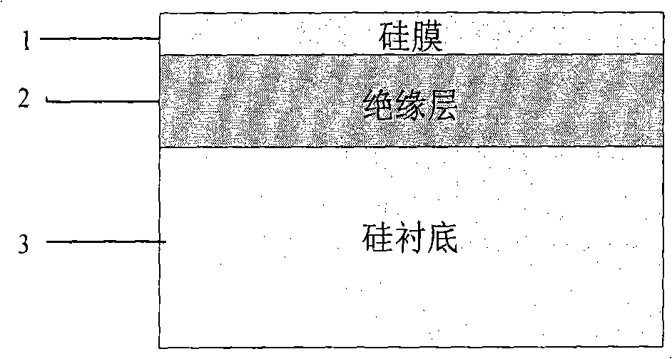
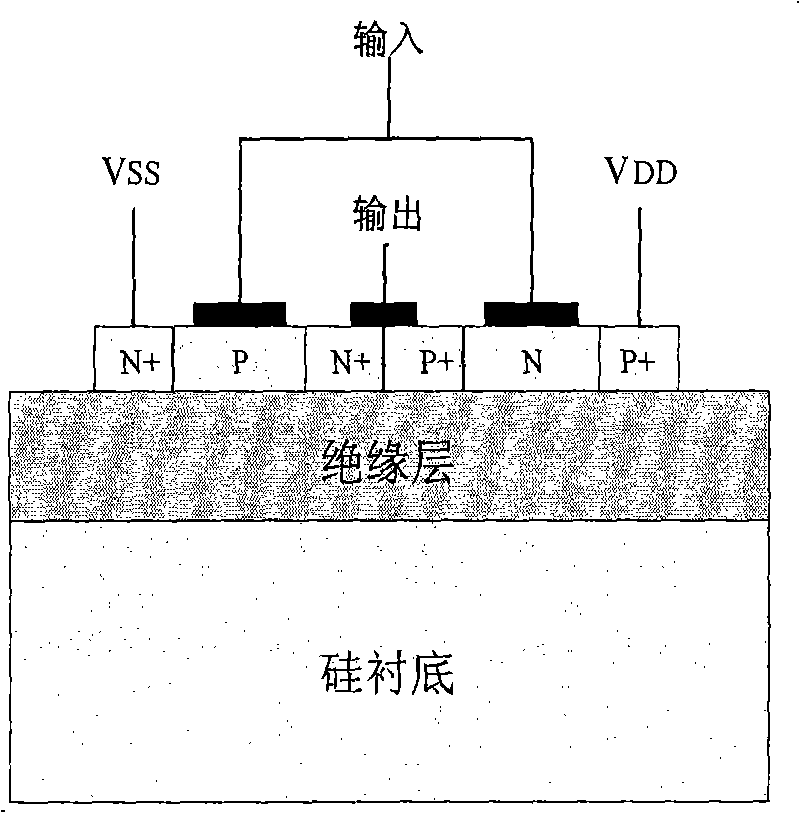
[0022] Figure 1 illustrates a starting SOI silicon wafer that can be used in the present invention. SOI silicon wafer It consists of top silicon film (1), insulating oxide layer (2) and silicon substrate (3). An SOICMOS circuit and N and PMOS devices for monitoring are prepared on the top silicon film (1). The SOI material is a commercial conventional oxygen ion implantation isolation (SIMOX) sheet, and other thermal bonding and smart-cut (Smart-Cut) sheets can also be used. For SOI CMOS circuits, the positive power supply voltage is applied to the source of the PMOS, and the ground potential (Vss) is applied to the source of the NMOS short.

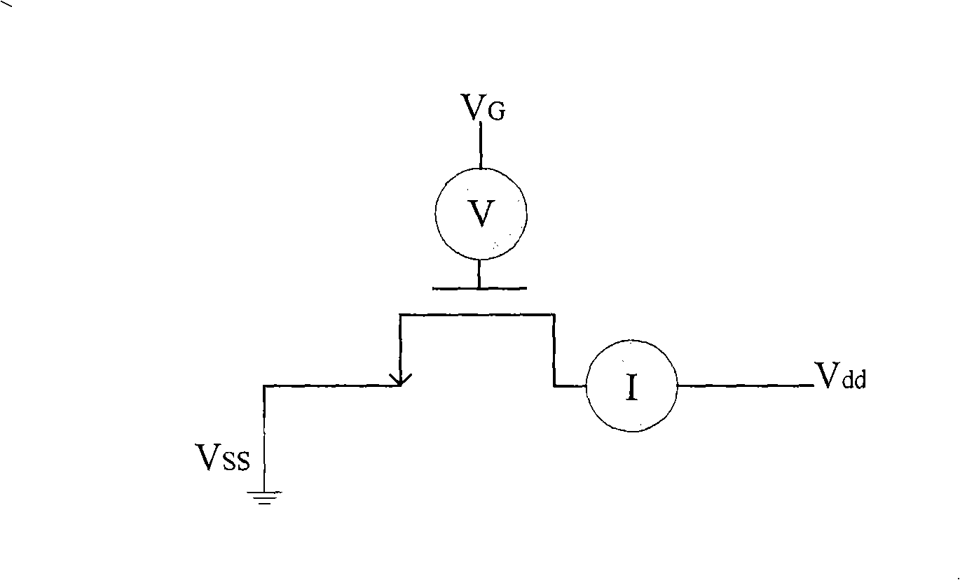
[0023] The invention relates to the bias of the back substrate of the SOI-CMOS integrated circuit, and provides the condition for charact...


PUM


Abstract

The present invention provides a method for testing a threshold voltage of a field effect transistor of the metal oxide semiconductor. The back substrate of the SOI-CMOS circuit is connected with an earth potential or an electric power potential, wherein, when the threshold voltage of the NMOS is tested, the back substrate is connected with the earth potential; and when the threshold voltage of the PMOS is tested, the back substrate is connected with the negative electric power potential. When the threshold voltage of the NMOS is tested, the back substrate is connected to the electric power potential; and when the threshold voltage of PMOS is tested, the back substrate is connected to the earth potential. The invention fixes the back substrate of SOI-CMOS circuit on a certain potential, and the operations of N, PMOS devices in SOI circuit are in back grid biases which are totally indifferent. Therefore, the condition for singly characterize the threshold voltage of N, PMOS should be altered correspondingly, and in this way the threshold voltage can be correctly recognized and controlled in order to guarantee the normal operation of SOI circuit.

Description

technical field [0001] The invention relates to an SOI-CMOS semiconductor integrated circuit, in particular to a substrate connection method during circuit packaging and an N-type or P-type metal oxide semiconductor field effect transistor (Metallic oxide semiconductor field effect transistor, NMOSEFT) in an SOI-CMOS semiconductor integrated circuit , PMOSEFT) threshold voltage test characterization method. Background technique [0002] SOI (Silicon-On-Insulator) technology refers to the fabrication of devices and circuits on a silicon film on an insulating layer (Box) (see Figure 1). Due to the existence of the buried oxide layer (Box), complete dielectric isolation is realized between devices, so the SOI-CMOS integrated circuit essentially avoids the latch-up effect of the bulk silicon CMOS circuit. In addition, the short channel effect of SOI devices is small, and shallow junctions can be formed naturally, and the leakage current is small. The small junction area result...

Claims


Application Information

Patent Timeline
Patent Type & Authority Applications(China)
IPC IPC(8): G01R31/26G01R31/28G01R19/00H01L21/66
Inventor 海潮和韩郑生周小茵赵立新李多力李晶
Owner INST OF MICROELECTRONICS CHINESE ACAD OF SCI
Why Eureka
Try Eureka