Substrate processing system and substrate cleaning apparatus

A technology for a substrate processing system and a substrate processing device, applied in chemical instruments and methods, cleaning methods and utensils, cleaning methods using liquids, etc., can solve the problem of semiconductor device quality degradation and possible reattachment on wafers (cross-contamination, failure Control problems such as pure water flow to achieve reliable removal

Inactive Publication Date: 2008-10-01
TOKYO ELECTRON LTD
View PDF1 Cites 40 Cited by
  • Summary
  • Abstract
  • Description
  • Claims
  • Application Information

AI Technical Summary

Problems solved by technology

As a result, there is a problem that the quality of semiconductor devices manufactured based on the wafer is lowered.
[0007] In addition, the wafers to be etched are transported in an airtight container (such as a front opening unified container (FOUP: wafer transfer box)) that holds a plurality of wafers parallel to each other. However, foreign objects (particles, polymers, etc.) ) is peeled off from the back surface or peripheral portion of the upper wafer, lands on the surface of the lower wafer and adheres thereto, degrading the quality of semiconductor devices manufactured based on the lower wafer
[0008] In addition, with the method of immersing a plurality of wafers in the above-mentioned cleaning tank, not only the particles on the surface of the wafers but also the particles on the back of the wafers and the inclined polymer on the peripheral portion of the wafers can be removed, but since the removed particles remain in the cleaning tank, In the liquid, the particles may reattach to the wafer (cross-contamination), reducing the quality of semiconductor devices
[0009] In addition, in the above-mentioned wet cleaning method, even if it is assumed that the particles and inclined polymers on the back surface of the wafer are removed, since the flow of pure water for wet cleaning cannot be controlled, the removed particles and the like are adjacent to the wafer being wet-cleaned, for example, it is possible Re-adhesion to the wafer surface that is wet-cleaned at the same time, deteriorating the quality of semiconductor devices

Method used


Image

  • Substrate processing system and substrate cleaning apparatus
  • Substrate processing system and substrate cleaning apparatus
  • Substrate processing system and substrate cleaning apparatus

Examples


Embodiment Construction

[0074] Hereinafter, embodiments of the present invention will be described with reference to the drawings.

[0075] First, a substrate processing system according to a first embodiment of the present invention will be described.

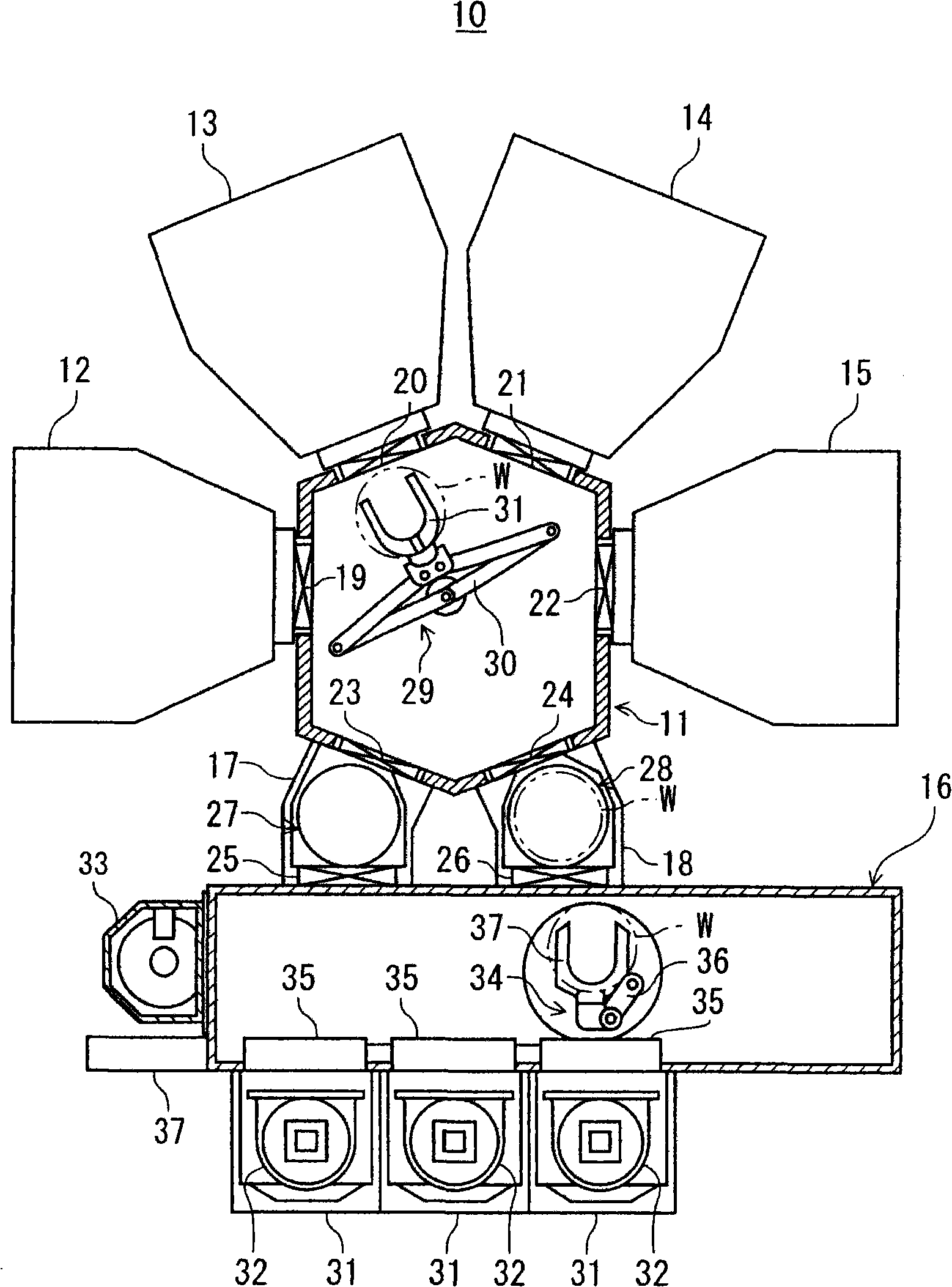
[0076] figure 1 It is a plan view schematically showing the structure of the substrate processing system of this embodiment.

[0077] exist figure 1 Among them, the substrate processing system 10 includes: a transfer module (transfer module) 11 that is hexagonal in plan view; four processing modules 12 to 15 arranged radially around the transfer module 11; a loading module that is a rectangular common transfer chamber 16; and two load lock assemblies 17, 18 arranged between the transfer assembly 11 and the loading assembly 16 for connecting the transfer assembly 11 and the loading assembly 16.

[0078] Each of the processing modules 12 to 15 is a substrate processing apparatus for performing predetermined processing on a wafer (hereinafter simply ...


PUM


Abstract

This invention provides a substrate processing system that enables foreign matter adhered to a rear surface or a periphery of a substrate to be completely removed. A processing assembly (15) of a substrate cleaning apparatus of the substrate processing system (10) including: a chamber (38) for accepting a wafer (W); a holding table (39) configured at the bottom of the chamber (38) and for placing the wafer W; a spray head configured at the top in the chamber (38) and opposite to the holding table (39).The holding table (39) jets the mixed cleaning agent of cleaning substrate (such as pure water) and inactive gas (such as N2) in two phases of a gas phase and a liquid phase at the back side or edge part facing to the wafer (W). The spray head (40) generates the down-flow facing to the surface of the wafer (W).

Description

technical field [0001] The present invention relates to a substrate processing system and a substrate cleaning device, and relates to a substrate processing system including a substrate cleaning device for removing foreign matter adhering to a back surface or a peripheral portion of a substrate. Background technique [0002] Generally, in a substrate processing apparatus that performs predetermined processing on a semiconductor wafer (hereinafter simply referred to as a "wafer") as a substrate, metal flakes (for example, aluminum metal flakes) or Reaction products (such as polymers of fluorocarbons) caused by the reaction of the process gas, etc. These foreign substances (particles) adhere to the wafer, deteriorating the quality of semiconductor devices formed on the surface of the wafer. [0003] As a method for removing particles adhering to a wafer, there is known a wet cleaning method in which an etched wafer is washed with hydrofluoric acid solution or pure water in a ...

Claims


Application Information

Patent Timeline
Patent Type & Authority Applications(China)
IPC IPC(8): H01L21/00H01L21/02H01L21/306B08B3/10B08B3/12
CPCH01L21/67051H01L21/6708H01L21/304
Inventor 守屋刚大西正野中龙西村荣一
Owner TOKYO ELECTRON LTD
Why Eureka
Try Eureka