Solid-state imaging device and imaging apparatus

一种固态成像装置、像素的技术,应用在辐射控制装置、固体图像信号发生器、带有单个拾取装置的信号发生器等方向,能够解决增加制造成本、装置构造复杂、难装置应用图像传感器等问题,达到改善质量的效果

Active Publication Date: 2008-10-08
SONY SEMICON SOLUTIONS CORP
View PDF1 Cites 20 Cited by
  • Summary
  • Abstract
  • Description
  • Claims
  • Application Information

AI Technical Summary

Problems solved by technology

However, this technique has substantial problems in that it is difficult to use the light entering the color image sensor sufficiently efficiently because the color filters themselves absorb light significantly.
In addition, this technique has the following problems: it is difficult to effectively use the pixels of the color image sensor because of spatial color separation; when the number of green pixels is small, the resolution of the luminance signal is reduced; When the number of is small, the resolution of the color signal is reduced, or a wrong color signal is produced
However, in this device, the color reproducibility is poor when utilizing the difference in absorption of light of different wavelengths in bulk silicon
For this reason, it is difficult to apply the device to the usual high-resolution image sensor
In addition, since the device configuration for extracting light corresponding to two colors through bulk silicon is complicated from a process point of view, the manufacturing cost is increased

Method used


Image

  • Solid-state imaging device and imaging apparatus
  • Solid-state imaging device and imaging apparatus
  • Solid-state imaging device and imaging apparatus

Examples


Embodiment Construction

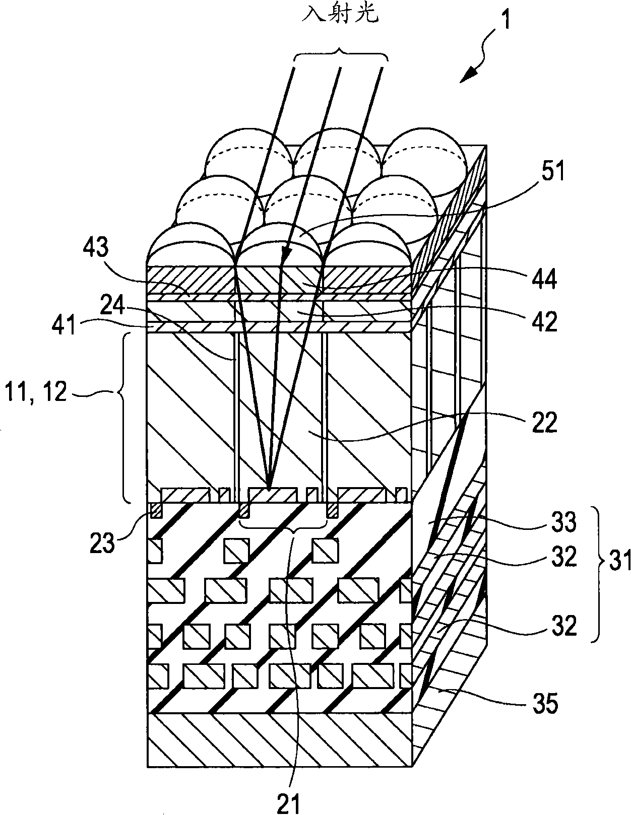
[0022] Now, will refer to figure 1 Schematic perspective view of the shown configuration and Figure 2A with 2B The layout diagram is shown to describe a solid-state imaging device according to an embodiment (first embodiment) of the present invention. refer to figure 1 , shows a whole-area-open-type CMOS image sensor as an application example of the solid-state imaging device according to the first embodiment of the present invention.

[0023] Such as figure 1 As shown, in the active layer 12 formed by the semiconductor substrate 11, a pixel unit 21 and a group of transistors 23 are formed, the pixel unit 21 includes a photoelectric conversion unit (for example, a photosensitive diode) 22, and each photoelectric conversion unit converts incident light converted into electrical signals, and a group of transistors 23 have transfer transistors, amplification transistors or reset transistors, etc. ( figure 1 A portion of the set of transistors 23 is shown in ). As the s...


PUM


Abstract

The present invention provides a solid-state imaging device and a imaging apparatus. The solid-state imaging device including a plurality of pixels that are provided on a semiconductor substrate, and that include a plurality of photoelectric-conversion units and metal oxide semiconductor transistors that selectively read signals from the plurality of photoelectric-conversion units, an organic-photoelectric-conversion film disposed on the plurality of photoelectric-conversion units, and an organic-color-filter layer disposed on the plurality of photoelectric-conversion units. Only a signal corresponding to a first color is extracted through the organic-photoelectric-conversion film. Signals corresponding to a plurality of colors not including the first color are extracted by absorption spectroscopy using the organic-color-filter layer.

Description

technical field [0001] The present invention relates to a solid-state imaging device and an imaging device. Background technique [0002] The semiconductor image sensor is a solid-state imaging device, and includes a complementary metal oxide semiconductor (CMOS) sensor and a charge coupled device (CCD). The CMOS sensor includes a plurality of pixels having a photoelectric conversion unit that converts incident light into an electrical signal, and a Metal Oxide Semiconductor (MOS) transistor that selectively reads the electrical signal from each pixel. The CCD includes a plurality of pixels having a photoelectric conversion unit that converts incident light into an electrical signal, which is read from each pixel through a silicon substrate, and transfers signal charges. Both CMOS sensors and CCDs are semiconductor devices that read signals from pixels. Recently, CMOS sensors have attracted attention as imaging devices used in cameras of mobile phones, digital still camera...

Claims


Application Information

Patent Timeline
Patent Type & Authority Applications(China)
IPC IPC(8): H01L27/146H04N5/225H01L27/14H04N9/07
CPCH01L27/14621H01L27/302H01L27/14627H01L27/307H04N9/045H04N25/13H04N25/17H01L27/146H04N23/12
Inventor 滝泽律夫名取太知
Owner SONY SEMICON SOLUTIONS CORP
Why Eureka
Try Eureka