

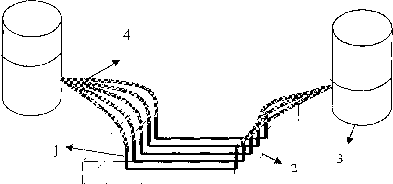
Process for preparing patterned cellulosic by micro-fluidic chip
A microfluidic chip, patterned technology, applied in microorganism-based methods, biochemical equipment and methods, microorganisms, etc., can solve problems such as not yet retrieved
- Summary
- Abstract
- Description
- Claims
- Application Information
AI Technical Summary
Problems solved by technology
Method used
Image

Examples
Embodiment 1
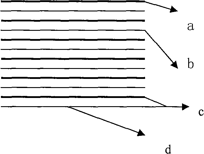
[0026] (1) Preparation of patterned positive film: preparation such as figure 2 For the photomask shown, uniformly coat a layer of photoresist SU8-GM1070 on the 2-stage polished silicon wafer with a glue throwing machine. The rotation speed of the glue throwing machine is set as: 500r / min, 30S; 1700r / min , 48S. A photoresist coating with a depth of 50 μm was thus obtained on the silicon wafer. The silicon wafer is pre-baked (first at 65°C for 15 minutes, then at 95°C for 2 hours), exposed to UV light for 85 seconds, post-baked (first at 65°C for 15 minutes, then at 95°C for 40 minutes), and developed with PGMEA for 2 minutes. Harden the film at 135°C for 2 hours to obtain patterned as figure 2 The positive membrane is shown. The anodic film pattern consists of thick and thin stripes, the thick stripe width a is 40 microns, the thin stripe width b is 20 microns, the stripe spacing c is 2 mm, and the stripe length d is 2 cm.
[0027] (2) Preparation of PDMS module: Stir th...
Embodiment 2
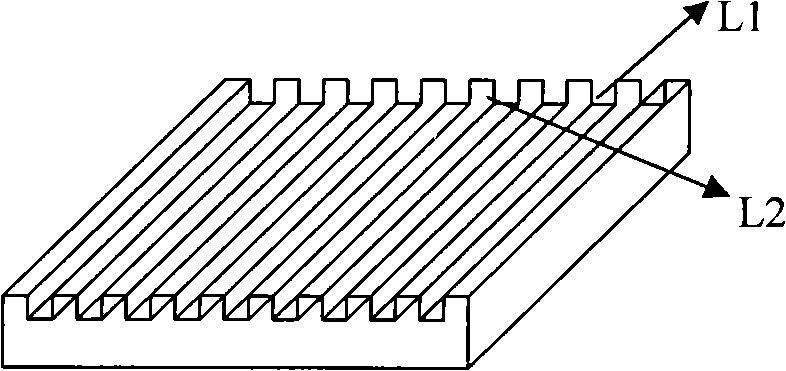
[0036](1) Preparation of patterned positive film: uniformly coat a layer of photoresist SU8-GM1070 on the 2-stage polished silicon wafer with a glue throwing machine, and set the rotation speed of the glue throwing machine as: 500r / min, 30S; 5000r / min, 48S. A photoresist coating with a depth of 15 μm was thus obtained on the silicon wafer. The silicon wafer is pre-baked (first at 65°C for 15 minutes, then at 95°C for 35 minutes), exposed to ultraviolet light for 35 seconds, post-baked (first at 65°C for 15 minutes, then at 95°C for 40 minutes), and developed with PGMEA for 25 seconds. After hardening the film at 135°C for 2 hours, the following Figure 4 The patterned positive film shown: the stripe width L1 is 20 μm, and the stripe spacing L2 is 40 μm.
[0037] (2) Preparation of PDMS module: Stir the mixture of Sylgard 184 silicone elastomer base and Sylgard184 silicone elastomer curing agent (5:1w / w) to vacuumize, pour it on the surface of the anodic membrane (thickness i...
Embodiment 3
[0046] (1) Preparation of patterned positive film: preparation such as Figure 6 For the photomask shown, uniformly coat a layer of photoresist SU8-GM1070 on the 2-stage polished silicon wafer with a glue throwing machine, and the rotation speed of the glue throwing machine is set as: 500r / min, 30S; 900r / min , 48S. A photoresist coating with a depth of 100 μm was thus obtained on the silicon wafer. The silicon wafer is pre-baked (first at 65°C for 15 minutes, then at 95°C for 2 hours), exposed to ultraviolet light for 100 seconds, post-baked (first at 65°C for 15 minutes, then at 95°C for 40 minutes), and developed with PGMEA for 7 minutes. Harden the film at 135°C for 2 hours to obtain Figure 6 The patterned positive film shown: the stripe width L1 is 50 μm, and the stripe spacing L2 is 200 μm.
[0047] (2) Preparation of PDMS module: Stir the mixture of Sylgard 184 silicone elastomer base and Sylgard184 silicone elastomer curing agent (10:1w / w) to vacuumize, pour it onto...
PUM
| Property | Measurement | Unit |
|---|---|---|
| depth | aaaaa | aaaaa |
| depth | aaaaa | aaaaa |
| width | aaaaa | aaaaa |
Abstract
Description
Claims
Application Information