Silicon wet method corrosion for manufacturing multiple stage micro-reflector

A technology of micro-reflector and wet etching, which is applied in the photoplate process of mirrors and patterned surfaces, optics, etc., and can solve problems such as difficulty in ensuring horizontal accuracy, difficulty in accurately controlling corrosion or etching depth, poor accuracy and repeatability, etc. , to achieve the effects of high flatness, improved production efficiency and precise control

Inactive Publication Date: 2010-10-27
CHANGCHUN INST OF OPTICS FINE MECHANICS & PHYSICS CHINESE ACAD OF SCI
View PDF1 Cites 1 Cited by
  • Summary
  • Abstract
  • Description
  • Claims
  • Application Information

AI Technical Summary

Problems solved by technology

Multi-level micro-mirrors can prepare step microstructures on various materials such as quartz by multiple photolithography and multiple etching (dry or wet) on the substrate by binary optical technology. This method has the following disadvantages: 1. Due to multiple overlays, the horizontal accuracy is difficult to guarantee; 2. It is difficult to accurately control the corrosion or etching depth, and the accuracy and repeatability are poor

Method used


Image

  • Silicon wet method corrosion for manufacturing multiple stage micro-reflector
  • Silicon wet method corrosion for manufacturing multiple stage micro-reflector
  • Silicon wet method corrosion for manufacturing multiple stage micro-reflector

Examples


Embodiment Construction

[0015] Combine below figure 1 with figure 2 The method of fabricating multi-level micro-mirrors by wet etching of silicon is introduced in detail.

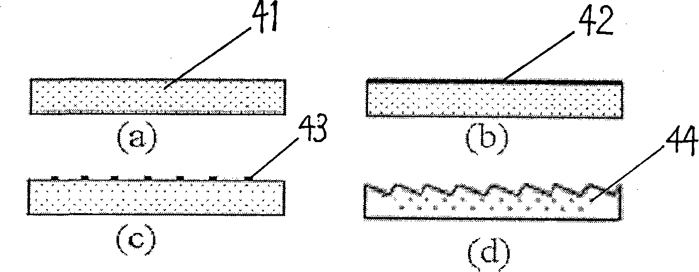
[0016] A, select the silicon chip 41 that upper surface and (111) face deviate certain angles as multistage microreflector material, polish its upper surface; Parameter setting, cleaning the silicon wafer after polishing.

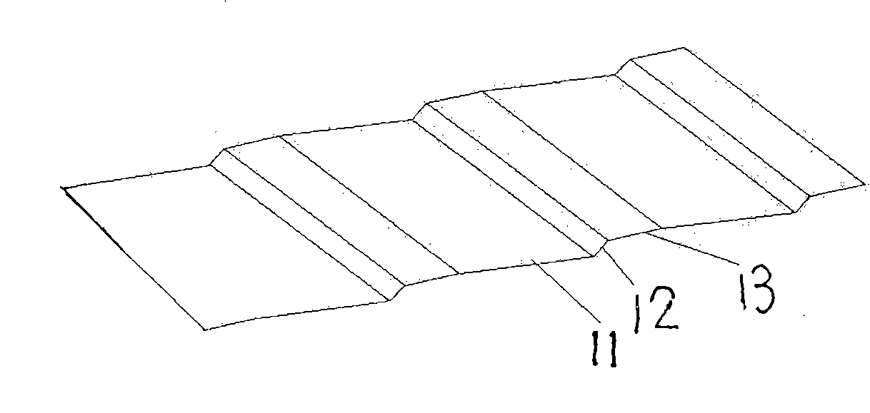
[0017] b. Design of photolithographic plate: design the photolithographic plate according to the design parameters of the multi-stage micro-reflector, the layout is bright and dark stripes; the width of the dark stripes is figure 2 The width of the midplane 13, the bright stripe width is figure 2 The width of the reflection surface 11 of the mid-level micro-mirror plus the projection of the truncated surface 12 on the upper surface of the silicon wafer 41 . Such as figure 2 As shown, both the reflective surface 11 and the truncated surface 12 are (111) surfaces of the silicon wafer, the angle between t...


PUM

PropertyMeasurementUnit
thicknessaaaaaaaaaa

Abstract

The invention relates to a method using silicon wet etching to produce a multi-stage microreflecting mirror, which comprises the following steps that: a silicon chip, the upper surface of which has certain angle with a (111) surface, is selected as a material of the multi-stage microreflecting mirror, and the upper surface of the silicon chip is polished; a layer of masking material grows on the surface of the silicon chip; a bar masking film pattern is formed on the upper surface of the silicon chip; the surface uncovered by the masking film undergoes anisotropic etching to obtain a staircase structure; and the surface of the staircase structure is coated with a reflection increasing film to obtain the multi-stage microreflecting mirror. One-time photoetching is adopted to obtain the masking film pattern and the particularity of the (111) surface of the silicon chip in the anisotropic etching technology is utilized to obtain a reflecting plane and a sectional surface of the multi-stage microreflecting mirror, so the method has small lateral dimension error during the production, can more accurately control the etching depth, and effective improve the longitudinal dimension accuracy and the repetitiveness of the staircase. The method has simple process and less process steps, and contributes to the improvement of production efficiency.

Description

technical field [0001] The invention relates to a method for manufacturing a multistage microreflector, in particular to a method for manufacturing a multistage microreflector by silicon wet etching. Background technique [0002] As a light reflection device, multistage micromirrors are widely used in optical systems, such as spectral analysis, beam shaping and fiber coupling. [0003] With the development of optical systems toward small size and compact structure, the miniaturization of devices in optical systems has become an important research topic for optical devices. The design and fabrication level of micro-optical devices directly determines the performance of optical instruments. Multi-level micro-mirrors can prepare step microstructures on various materials such as quartz by multiple photolithography and multiple etching (dry or wet) on the substrate by binary optical technology. This method has the following disadvantages: 1. Due to multiple overlays, the horizon...

Claims


Application Information

Patent Timeline
Patent Type & Authority Patents(China)
IPC IPC(8): G02B5/08G03F7/00G02B1/10G02B1/14
Inventor 梁静秋梁中翥禹秉熙
Owner CHANGCHUN INST OF OPTICS FINE MECHANICS & PHYSICS CHINESE ACAD OF SCI
Why Eureka
Try Eureka