Manufacturing method of grid dielectric layer and grid

A gate dielectric layer and manufacturing method technology, which is applied in the field of semiconductor manufacturing, can solve the problems of semiconductor device stability and electrical performance degradation, dense silicon oxide layer insulation capacity degradation, uniformity deterioration, etc., to achieve stable and consistent electrical characteristics , high carrier mobility and turn-on sensitivity, good uniformity

Inactive Publication Date: 2008-10-22
SEMICON MFG INT (SHANGHAI) CORP
View PDF1 Cites 14 Cited by
  • Summary
  • Abstract
  • Description
  • Claims
  • Application Information

AI Technical Summary

Problems solved by technology

The uniformity of the thickness of the silicon oxide layer becomes worse, the density decreases and the defects increase, all of which will cause the insulation capacity of the silicon oxide layer to decrease

Method used


Image

  • Manufacturing method of grid dielectric layer and grid
  • Manufacturing method of grid dielectric layer and grid
  • Manufacturing method of grid dielectric layer and grid

Examples


Embodiment Construction

[0039] The specific embodiments of the present invention will be described in detail below in conjunction with the accompanying drawings.

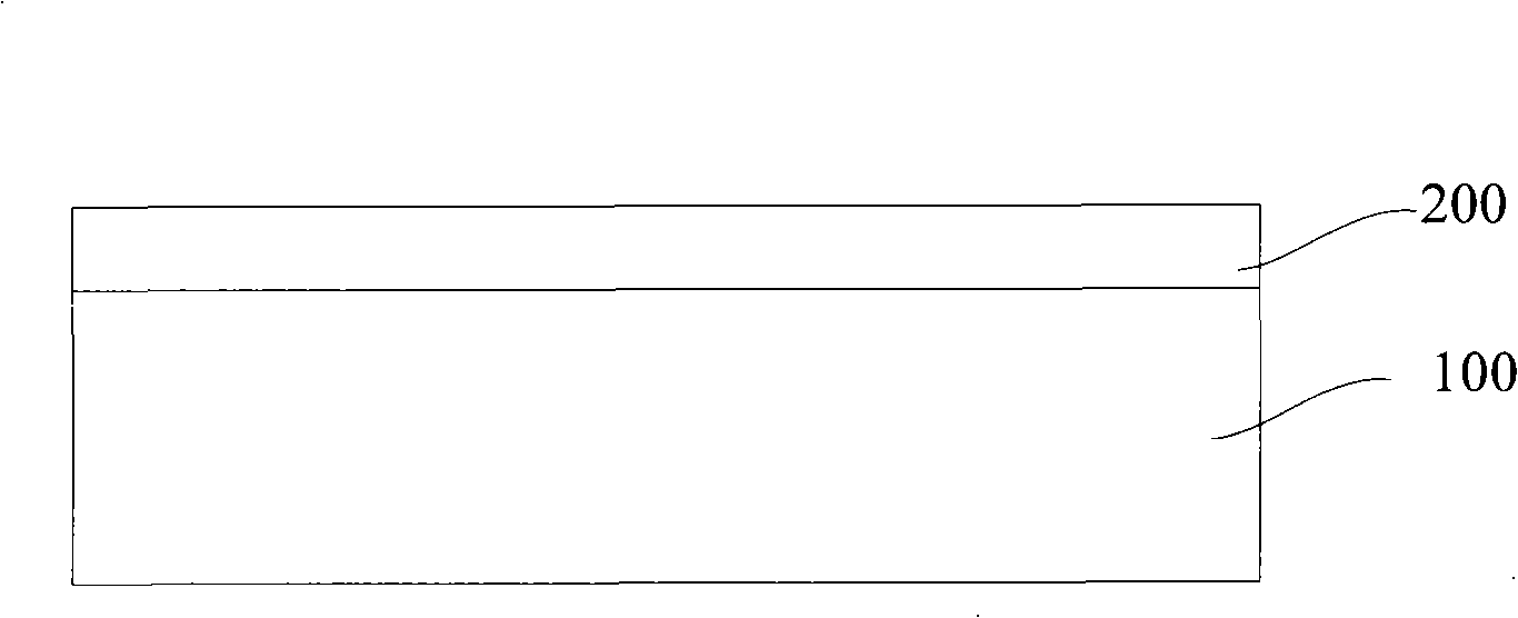
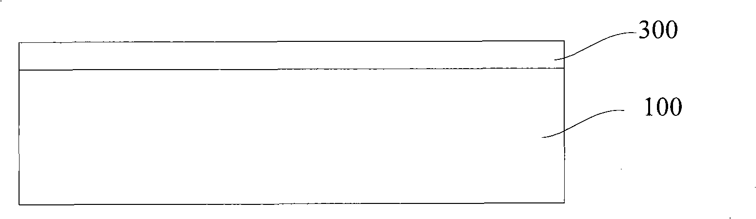
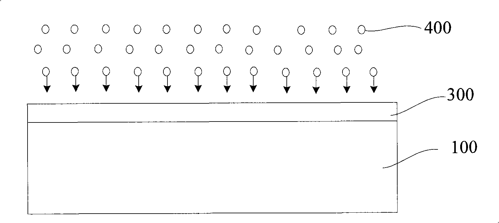
[0040] With the development of semiconductor manufacturing technology, the size of the gate is getting smaller and smaller, and the operating voltage acting on the gate also needs to be reduced accordingly. In order to ensure the fast response characteristics of the formed semiconductor device, the thickness of the corresponding gate dielectric layer Thinning is also required as gate dimensions continue to decrease. Generally speaking, the ratio of the size of the gate to the gate dielectric layer corresponding to the gate is about 45 to 50, which means that when the gate size is reduced to 65nm or even smaller, the gate dielectric layer corresponding to the gate The thickness of the layer should be less than 1.5 nm. This is a big challenge to the existing process for forming the gate dielectric layer. The invention provides a method for...


PUM


Abstract

A method for making a gate medium layer comprises the following steps that: a semiconductor substrate is provided; nitrogen treatment of the surface of the semiconductor substrate is carried out; and oxidation process of the surface of the semiconductor substrate is carried out after the nitrogen treatment so as to form an oxygenous medium layer. The invention also provides a method for making a grid electrode. The gate medium layer formed through the method has thinner thickness and better thickness evenness.

Description

technical field [0001] The invention relates to the technical field of semiconductor manufacturing, in particular to a method for manufacturing a gate dielectric layer and a gate. Background technique [0002] Since the invention of the metal oxide semiconductor transistor, silicon oxide has been used as the most important material of the gate dielectric layer due to its good integration characteristics with silicon and polysilicon. With the improvement of integration, the size of the gate is getting smaller and smaller. Correspondingly, the thickness of the silicon oxide layer as the gate dielectric layer also needs to be continuously reduced, which has a great impact on the thickness uniformity and defect control of the formed silicon oxide layer. The requirements for the characteristics of the film layer are getting higher and higher, which puts forward higher requirements for the manufacturing process of the silicon oxide layer. The silicon oxide layer formed by the exis...

Claims


Application Information

Patent Timeline
IPC IPC(8): H01L21/314H01L21/28H01L21/336
Inventor 虞肖鹏
Owner SEMICON MFG INT (SHANGHAI) CORP
Why Eureka
Try Eureka