Semi-penetrating semi-reflective liquid crystal display device and manufacturing method thereof

A semi-transmissive semi-reflective, liquid crystal display panel technology, applied in semiconductor/solid-state device manufacturing, semiconductor devices, optics, etc., can solve the complex process, difficulty in subsequent brushing and alignment patterns, and difficulty in arranging spacers for liquid crystal gap height control, etc. problems, to achieve the effect of simplifying the process, increasing the aperture ratio, and increasing the area

Active Publication Date: 2008-10-29
AU OPTRONICS CORP
View PDF0 Cites 8 Cited by
  • Summary
  • Abstract
  • Description
  • Claims
  • Application Information

AI Technical Summary

Problems solved by technology

First of all, it is known that the transflective liquid crystal display panel must use at least eight lithography processes to define the semiconductor layer, source / drain, lightly doped drain, gate, and the first interlayer dielectric layer respectively. , data line and drain connection pad, the second interlayer dielectric layer, the pattern of the penetrating electrode and the reflective electrode, so the process is more complicated
In addition, because the reflective area is provided with the second interlayer dielectric layer, but the penetrating area is not provided with the second interlayer dielectric layer, so that there is a height difference between the reflective area and the penetrating area, and this height difference is likely to cause subsequent brushing. The difficulty of rubbing the alignment pattern, and in the subsequent liquid crystal process, it will also cause the difficulty of controlling the height of the liquid crystal gap (Cell Gap) and the arrangement of the spacer (spacer)

Method used


Image

  • Semi-penetrating semi-reflective liquid crystal display device and manufacturing method thereof
  • Semi-penetrating semi-reflective liquid crystal display device and manufacturing method thereof
  • Semi-penetrating semi-reflective liquid crystal display device and manufacturing method thereof

Examples


Embodiment Construction

[0040]In order for those skilled in the art to have a better understanding of the present invention, several preferred embodiments of the present invention are enumerated below, together with the accompanying drawings, to describe in detail the composition and desired effects of the present invention.

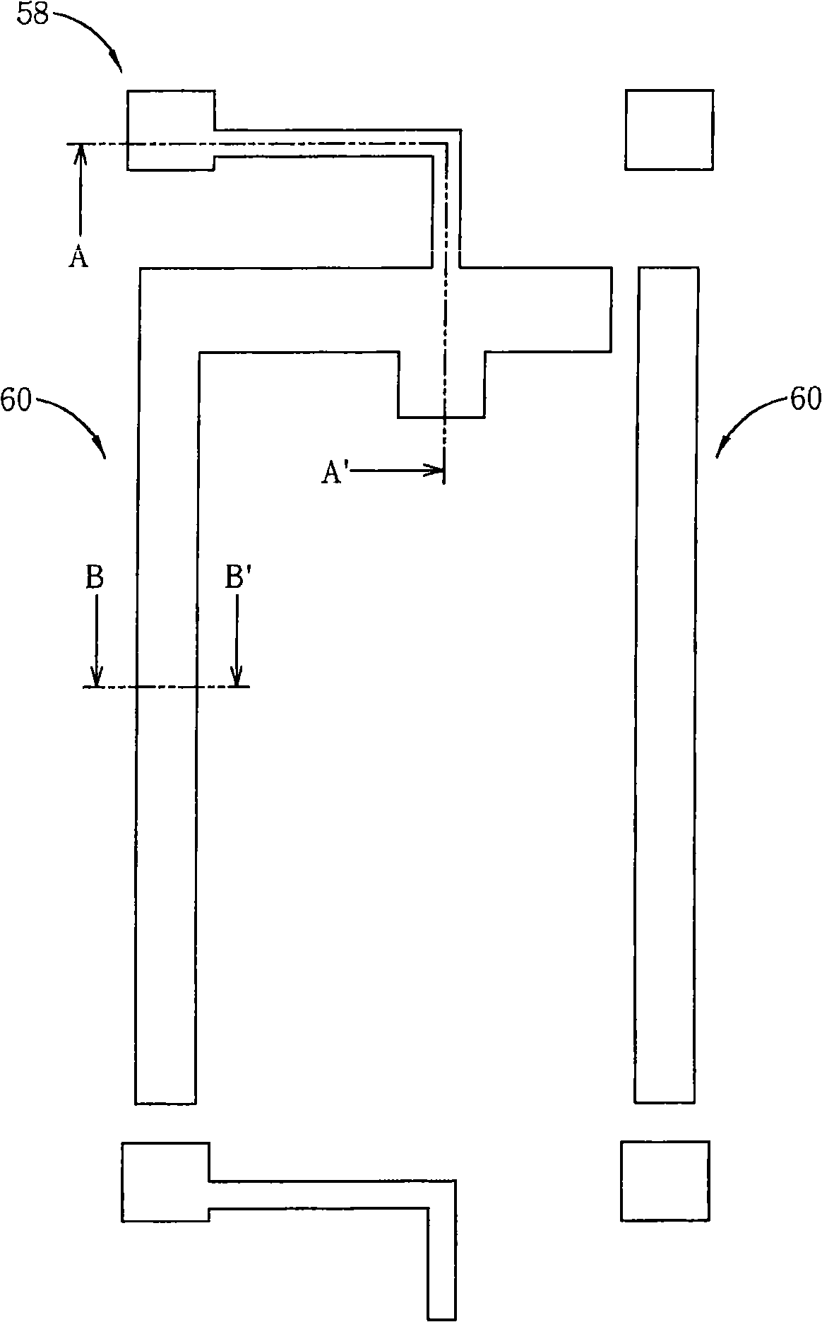
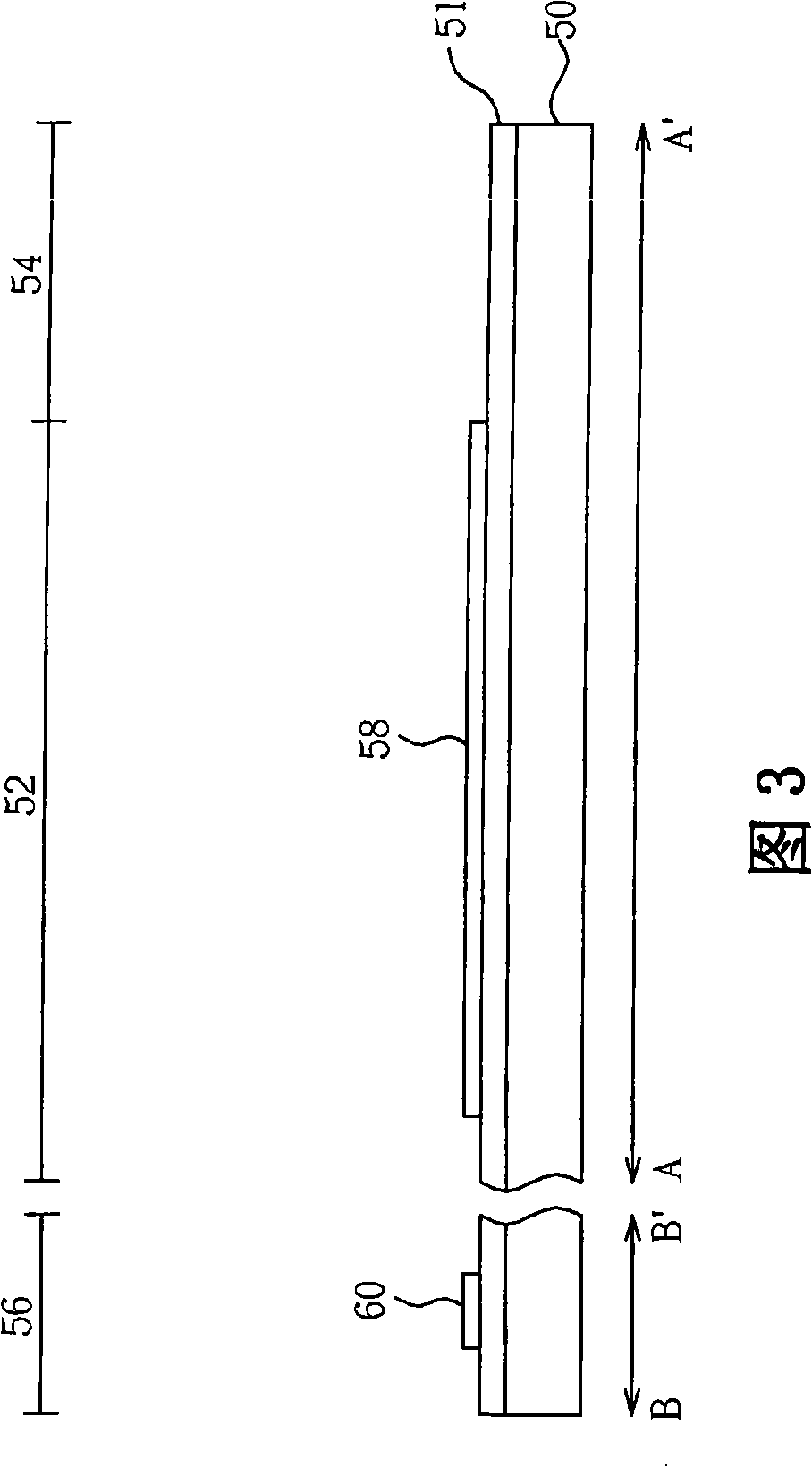
[0041] Please refer to figure 2 to Figure 17. figure 2 17 is a schematic diagram of a method for manufacturing a preferred embodiment of the transflective liquid crystal display panel of the present invention. For ease of illustration, only one pixel area is shown in the drawings, and figure 2 , Figure 4 , Figure 6 , Figure 8 , Figure 10 , Figure 12 , Figure 14 and Figure 16 3, 5, 7, 9, 11, 13, 15 and 17 are schematic cross-sectional views of the pixel region along the section lines AA' and BB'. Such as figure 2 As shown in FIG. 3 , firstly, a substrate 50 is provided, and a reflective region 52 , a transmissive region 54 and a peripheral region 56 are defined ...


PUM


Abstract

The invention provides a transflective liquid crystal display panel and a manufacturing method thereof. The display panel comprises a substrate, a first polycrystalline silicon pattern arranged in a pixel reflecting area, a second polycrystalline silicon pattern arranged in a pixel peripheral area, insulating layers arranged on the first polycrystalline silicon pattern, the second polycrystalline silicon pattern and the substrate, a grid arranged on the insulating layer of the pixel reflecting area, a common electrode arranged on the insulating layer of the pixel peripheral area, a first interlayer dielectric layer arranged on the insulating layers, the grid and the common electrode, a reflecting electrode arranged on the first interlayer dielectric layer, a second interlayer dielectric layer arranged on the first interlayer dielectric layer and the reflecting electrode, and a penetrating electrode arranged on the second interlayer dielectric layer and electrically connected with the reflecting electrode by penetrating the opening of the second interlayer dielectric layer; a storing capacitance is formed by the second polycrystalline silicon pattern, the common electrode and the insulating layers between the second polycrystalline silicon pattern and the common electrode; the reflecting electrode is arranged above a thin film transistor so as to increase the area of the reflecting area; and the storing capacitance is arranged under a data line so as to promote the aperture ratio.

Description

technical field [0001] The invention relates to a semi-transmitting and semi-reflecting liquid crystal display panel and a manufacturing method thereof, in particular to a semi-transmitting and semi-reflecting liquid crystal display panel with a high aperture ratio and simple process and a manufacturing method thereof. Background technique [0002] According to different sources of illumination light, liquid crystal displays can be divided into three types: transmissive, reflective, and transflective. The transmissive liquid crystal display requires a backlight module for generating light on the back of the liquid crystal display panel, and the light generated by the light will pass through the liquid crystal display panel so that the viewer can watch the picture display of the liquid crystal display from the front. The reflective LCD uses ambient light as the light source, and reflective electrodes need to be set in the pixel area; when the reflective LCD displays a picture...

Claims


Application Information

Patent Timeline
IPC IPC(8): G02F1/1335G02F1/1362H01L27/12H01L21/84
Inventor 陈昱丞杨敦钧
Owner AU OPTRONICS CORP
Why Eureka
Try Eureka