Manufacturing method of semiconductor device

A manufacturing method and semiconductor technology, applied in semiconductor/solid-state device manufacturing, electrical components, circuits, etc., can solve problems such as difficulty in suppressing short-channel effects of devices, lack of impurities, and degradation of input/output device life, so as to reduce heat load Jet injection effect, optimized performance, and the effect of not degrading short channel characteristics

Active Publication Date: 2010-04-21
SEMICON MFG INT (SHANGHAI) CORP
View PDF4 Cites 0 Cited by
  • Summary
  • Abstract
  • Description
  • Claims
  • Application Information

AI Technical Summary

Problems solved by technology

[0009] However, the manufacturing method of the above-mentioned semiconductor device has the following disadvantages: 1) there is only one low-doped source-drain region ion implantation, which is difficult to suppress the short channel effect that occurs after the device is continuously reduced; 2) the low-doped source-drain of the input / output device After ion implantation in the region, there is no annealing to fully activate and diffuse impurities, which can cause the low-doped source region at the drain to form a high-intensity electric field under the gate dielectric layer, resulting in hot carrier effects, resulting in serious degradation of the life of the input / output device

Method used


Image

  • Manufacturing method of semiconductor device
  • Manufacturing method of semiconductor device
  • Manufacturing method of semiconductor device

Examples


Embodiment 1

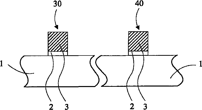
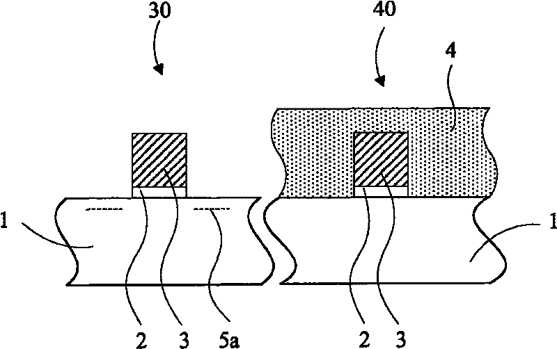
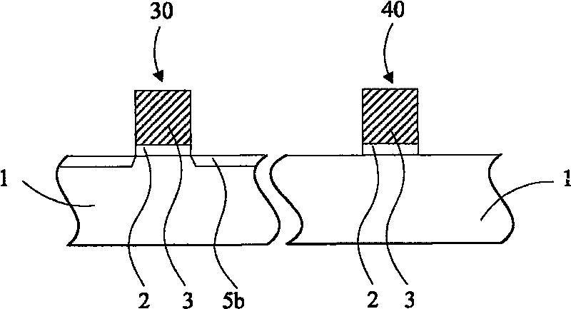
[0048] This embodiment provides a method for manufacturing a semiconductor device, refer to the attachment Figure 14 As shown in the process flow chart, it includes the following steps: step S200, a semiconductor substrate is provided, the semiconductor substrate includes a core device area and an input / output device area, the core device area and the input / output device area are both formed on the semiconductor substrate The gate dielectric layer and the gate located on the gate dielectric layer; step S210, using the gate as a mask, perform the first ion implantation in the semiconductor substrate in the core device area; step S220, perform sharp annealing, Low-doped source and drain regions are formed in the semiconductor substrate on both sides of the gate dielectric layer in the core device region; step S230, using the gate as a mask, perform a second ion implantation into the semiconductor substrate in the input / output device region Step S240, perform rapid thermal anneali...

Embodiment 2

[0093] This embodiment provides a method for manufacturing a semiconductor device, including the following steps:

[0094] In step S300, a semiconductor substrate is provided. The semiconductor substrate includes a core device area and an input / output device area. A gate dielectric layer and a gate dielectric layer are formed on the semiconductor substrate in the core device area and the input / output device area. The gate on the layer has a first spacer formed on the gate dielectric layer of the core device area and the sidewall of the gate;

[0095] Step S310, using the first spacer as a mask, perform the first ion implantation into the semiconductor substrate in the core device area;

[0096] Step S320, performing sharp annealing to form low-doped source and drain regions in the semiconductor substrate on both sides of the first spacer in the core device region;

[0097] Step S330, using the gate as a mask, perform a second ion implantation into the semiconductor substrate in the in...


PUM


Abstract

A manufacture method for a semiconductor apparatus includes the following steps of: providing a semiconductor underlay which consists of a core apparatus area and an I / O area and is formed with a griddielectric layer and a grid arranged on the grid dielectric layer; carrying out a first ion injection in the semiconductor underlay of the core apparatus area by taking the grid as a mask; carrying out spike annealing and forming a low doping source drain area in the core apparatus area; carrying out a secondary ion injection in the semiconductor underlay of the I / O area by taking the grid as themask; carrying out fast thermal annealing and forming a low doping source drain area in the I / O area; forming a clearance wall on the grid dielectric layer of the core apparatus area and the I / O areaaswell as the side wall of the grid; carrying out a third ion injection in the semiconductor underlay of the core apparatus area and the I / O area by taking the grid and the clearance wall as the masksto form a heavy doping source drain area. The method can adjust the saturation current of an apparatus and improve the reliability of input / output apparatuses.

Description

Technical field [0001] The present invention relates to the field of semiconductor technology, in particular to a manufacturing method of a semiconductor device. Background technique [0002] With the rapid development of semiconductor manufacturing technology, in order to achieve faster computing speed, greater data storage capacity and more functions, semiconductor chips are developing towards higher device density and high integration. Most of the peripheral circuits of semiconductor chips need to use high-voltage input / output devices, while core devices such as various memory devices need to operate at low voltages. In order to maximize device performance, the channel length of the core devices has become shorter, resulting in short Channel region and short channel effect. In order to avoid the short channel effect, a lightly doped source / drain (LDD) structure is usually adopted. [0003] As the channel length of the core device shrinks, in order to obtain the required drive ...

Claims


Application Information

Patent Timeline
Patent Type & Authority Patents(China)
IPC IPC(8): H01L21/8234
Inventor 赵猛
Owner SEMICON MFG INT (SHANGHAI) CORP
Why Eureka
Try Eureka