Preparing method of p-type stannous oxide ditch film transistors

A thin-film transistor and tin oxide technology, which is applied in semiconductor/solid-state device manufacturing, ion implantation plating, coating, etc., can solve the problems of low field effect mobility, high preparation difficulty, and high preparation cost, and achieve high field Effect mobility, simple preparation process, and reduced difficulty of device preparation

Inactive Publication Date: 2010-06-30
NINGBO INST OF MATERIALS TECH & ENG CHINESE ACADEMY OF SCI
View PDF0 Cites 33 Cited by
  • Summary
  • Abstract
  • Description
  • Claims
  • Application Information

AI Technical Summary

Problems solved by technology

However, the field effect mobility of the p-type TFT with tin oxide and nickel oxide as the channel layer is very low, less than 0.011 cm 2 V -1 the s -1 ; Although the field-effect mobility of the p-type TFT with stannous oxide as the channel layer is two orders of magnitude higher than that of the former two, its channel layer is made of expensive yttria-stabilized zirconia (yttria-stabilizedzirconia, The SnO epitaxial film is prepared on the YSZ)(001) subst

Method used


Image

  • Preparing method of p-type stannous oxide ditch film transistors
  • Preparing method of p-type stannous oxide ditch film transistors
  • Preparing method of p-type stannous oxide ditch film transistors

Examples


Embodiment Construction

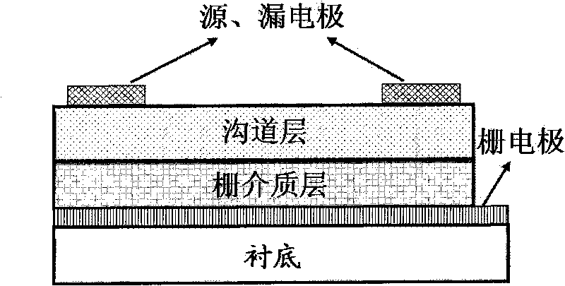
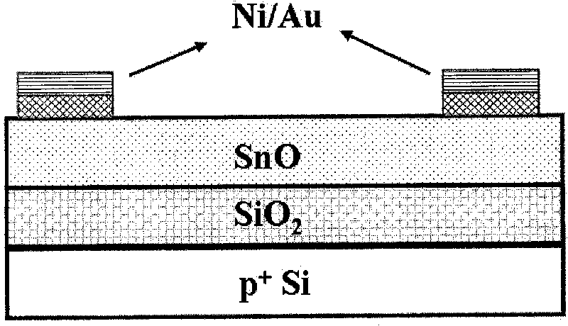
[0035] This example describes the SiO 2 p-type SnO channel thin film transistor with bottom gate structure prepared on / Si substrate (such as image 3 shown), and a comparative analysis of the performance of transistors annealed at 300°C to 450°C was performed.

[0036] Step 1: Select Commercially Purchased Thermally Oxidized Silicon Wafer SiO 2 / p + -Si(100) as substrate with SiO 2 layer as a gate dielectric layer with a thickness of 190nm, while p-type highly doped p + -Si substrate can also be used as gate electrode;

[0037] Step 2: Using electron beam evaporation equipment and tin oxide evaporation material, deposit a 100nm stannous oxide amorphous film on the gate dielectric layer at room temperature, and then perform thermal annealing treatment in an Ar gas atmosphere, and the annealing temperature is 300 ℃~ 450℃, one temperature point per 50℃, annealing time is 10min;

[0038] Step 3: Ni / Au source electrode and Ni / Au drain electrode are prepared by electron beam ...


PUM


Abstract

The present invention discloses a preparing method of p-type stannous oxide ditch film transistors, and p-type conducting stannous oxide ditch layers are prepared by using electron beam evaporation technology and rapid thermal annealing technology. The preparing method is simple and controllable, and can realize low-temperature preparation. The p-type stannous oxide ditch film transistors have high field effect mobility, can be used for organic light-emitting diodes and development of oxide based compensating and logic circuits with low loss and the like, and have wide application prospects in the technical field of displays.

Description

technical field [0001] The invention relates to a preparation method of a thin film transistor, in particular to a preparation method of a p-type stannous oxide channel thin film transistor. Background technique [0002] Thin film transistors (TFTs) are generally composed of substrates, gate dielectric layers, channel layers, gate electrodes, source electrodes and drain electrodes, including TFTs with bottom gate structures (such as figure 1 shown) and top-gate TFTs (such as figure 2 shown), it is used as a switching element in liquid crystal displays to drive pixels, in which Si-based (amorphous Si or polycrystalline Si is the channel) TFT is dominant, but both amorphous Si TFT and polycrystalline Si TFT have irreversible Disadvantages to be overcome, such as photoinduced performance degradation, lower field-effect mobility, limited aperture ratio, and higher power consumption. Therefore, the development of display technology objectively requires the replacement of Si ma...

Claims


Application Information

Patent Timeline
IPC IPC(8): H01L21/34H01L21/477C23C14/24
Inventor 曹鸿涛梁凌燕刘志敏
Owner NINGBO INST OF MATERIALS TECH & ENG CHINESE ACADEMY OF SCI
Why Eureka
Try Eureka