Field effect transistor having field plate electrodes
A technology of field effect transistors and semiconductors, which is applied in the direction of semiconductor devices, electrical components, circuits, etc., can solve the problem of FET high-frequency gain characteristics decline, and achieve the effect of improving high-frequency gain characteristics
- Summary
- Abstract
- Description
- Claims
- Application Information
AI Technical Summary
Problems solved by technology
Method used
Image

Examples
Embodiment approach 1
[0024] Hereinafter, a structure of a field effect transistor according to an embodiment of the present invention will be described with reference to the drawings. In addition, each drawing only schematically shows the shape, size, and arrangement relationship of each structural element so that the present invention may be understood. In addition, preferred structural examples of the present invention are described below, but the materials, numerical conditions, and the like of each structural element are merely preferred examples. Therefore, the present invention is not limited to any of the following embodiments.
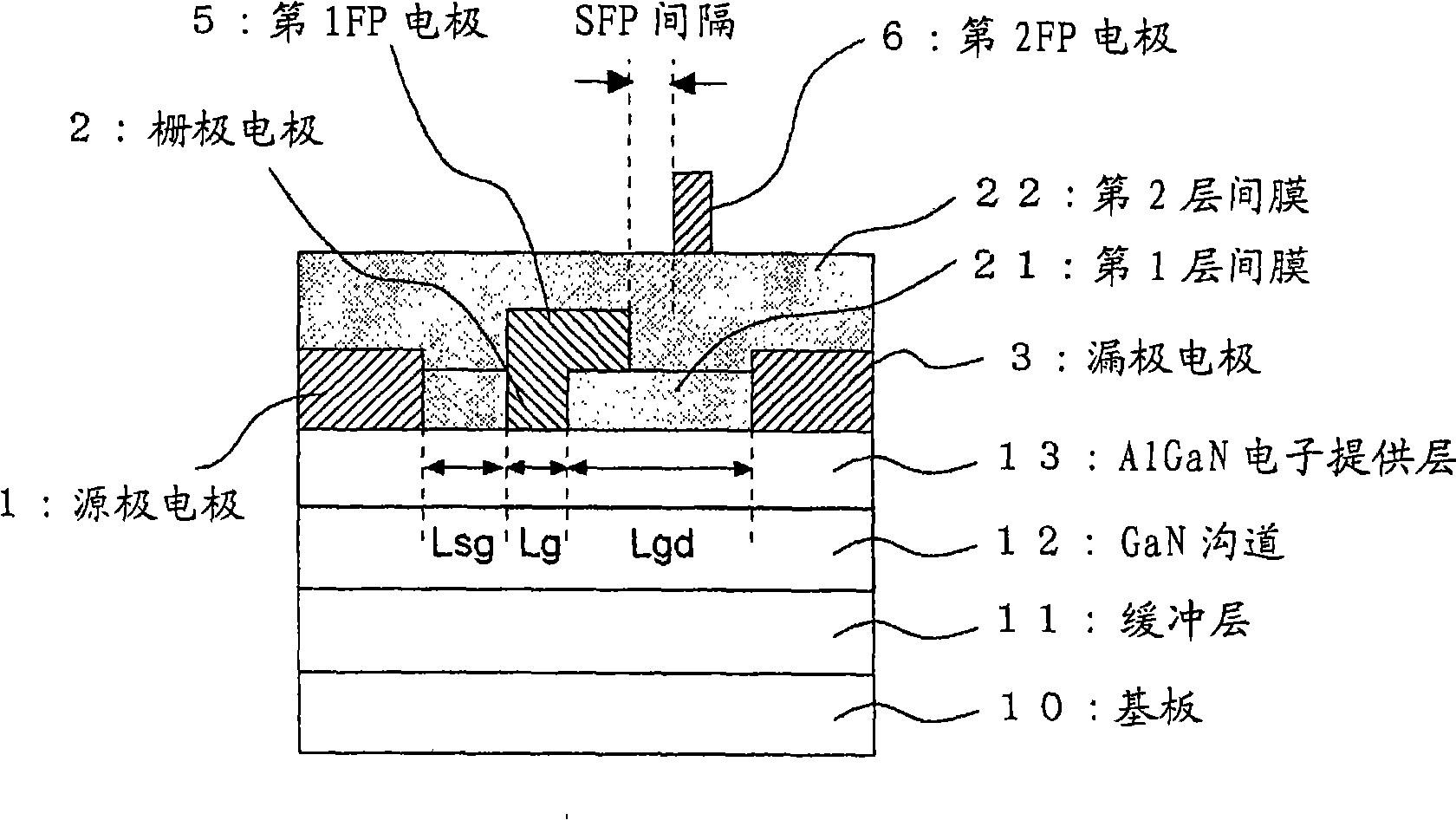
[0025] Regarding the field effect transistor of Embodiment 1, a structure of a high electron mobility transistor (HEMT: High Electron Mobility Transistor, hereinafter referred to as "GaN-HEMT") having an active layer made of an AlGaN / GaN heterostructure will be described. In addition, the present invention is not limited thereto, and may be a GaAs field effect tra...
Embodiment approach 2
[0067] In the first embodiment described above, the case where the first FP electrode 5 is integrally formed with the gate electrode 2 was described, but in the second embodiment, an example is shown in which the first FP electrode 5 is connected to the gate electrode 2 via a wiring outside the FET. .
[0068] Figure 7 It is a sectional view showing the structure of the field effect transistor of Embodiment 2. like Figure 7 As shown, the first FP electrode 5 of the second embodiment is formed separately from the gate electrode 2 and is connected to the gate electrode 2 through a wiring layer. The first FP electrode 5 is provided on the first interlayer film 21 in the region between the gate electrode 2 and the drain electrode 3 . Furthermore, the second FP electrode 6 is provided in the region between the first FP electrode 5 and the drain electrode 3 as in the first embodiment described above. The other structures and device dimensions are the same as those in the first...
Embodiment approach 3
[0071] In Embodiment 1 described above, the case where the first FP electrode 5 is integrally formed with the gate electrode 2 is described, but in Embodiment 3, an example in which the first FP electrode 5 is covered and connected with the gate electrode 2 is shown.
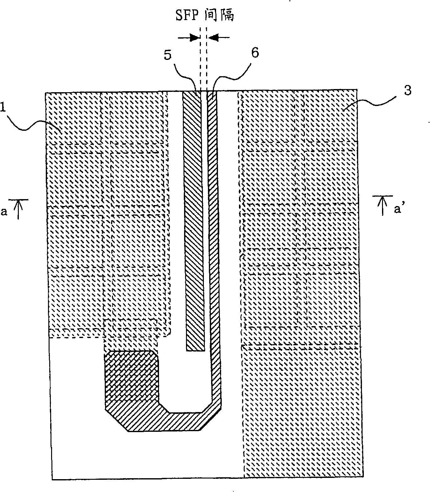
[0072] Figure 8 It is a sectional view showing the structure of the field effect transistor of Embodiment 3. Figure 9 It is a top view explaining the structure of the field effect transistor of Embodiment 3. in addition, Figure 9 express Figure 8 The a-a' profile in . exist Figure 8 and Figure 9 In the third embodiment, the first FP electrode 5 is formed of a metal different from that of the gate electrode 2 . For example, Ni / Au is used for the gate electrode 2 and Ti / Pt / Au is used for the first FP electrode 5 . And, the first FP electrode 5 is covered and connected to the gate electrode 2 . Also, as shown in the figure, the first FP electrode 5 is provided on the first interlayer film 21 in the re...
PUM
 Abstract
Description
Claims
Application Information
PatSnap Eureka turns technology decisions into work you can execute. Powered by our Innovation Knowledge Graph, it runs expert workflows across engineering, life sciences, materials and intellectual property. Get your review-ready output in minutes.


