Flip LED integrated chip with high break-over voltage

An integrated chip, high-conductivity technology, used in semiconductor/solid-state device manufacturing, circuits, electrical components, etc., can solve problems such as poor high-voltage resistance performance of LED integrated chips, and achieve a small footprint, low manufacturing cost, and wide distribution area. Effect

Inactive Publication Date: 2008-11-19
NANKER GUANGZHOU SEMICON MFG
View PDF0 Cites 17 Cited by
  • Summary
  • Abstract
  • Description
  • Claims
  • Application Information

AI Technical Summary

Problems solved by technology

Therefore, the high-voltage resistance performance of the existing LED integrated chip is not good

Method used


Image

  • Flip LED integrated chip with high break-over voltage
  • Flip LED integrated chip with high break-over voltage
  • Flip LED integrated chip with high break-over voltage

Examples


Embodiment 1

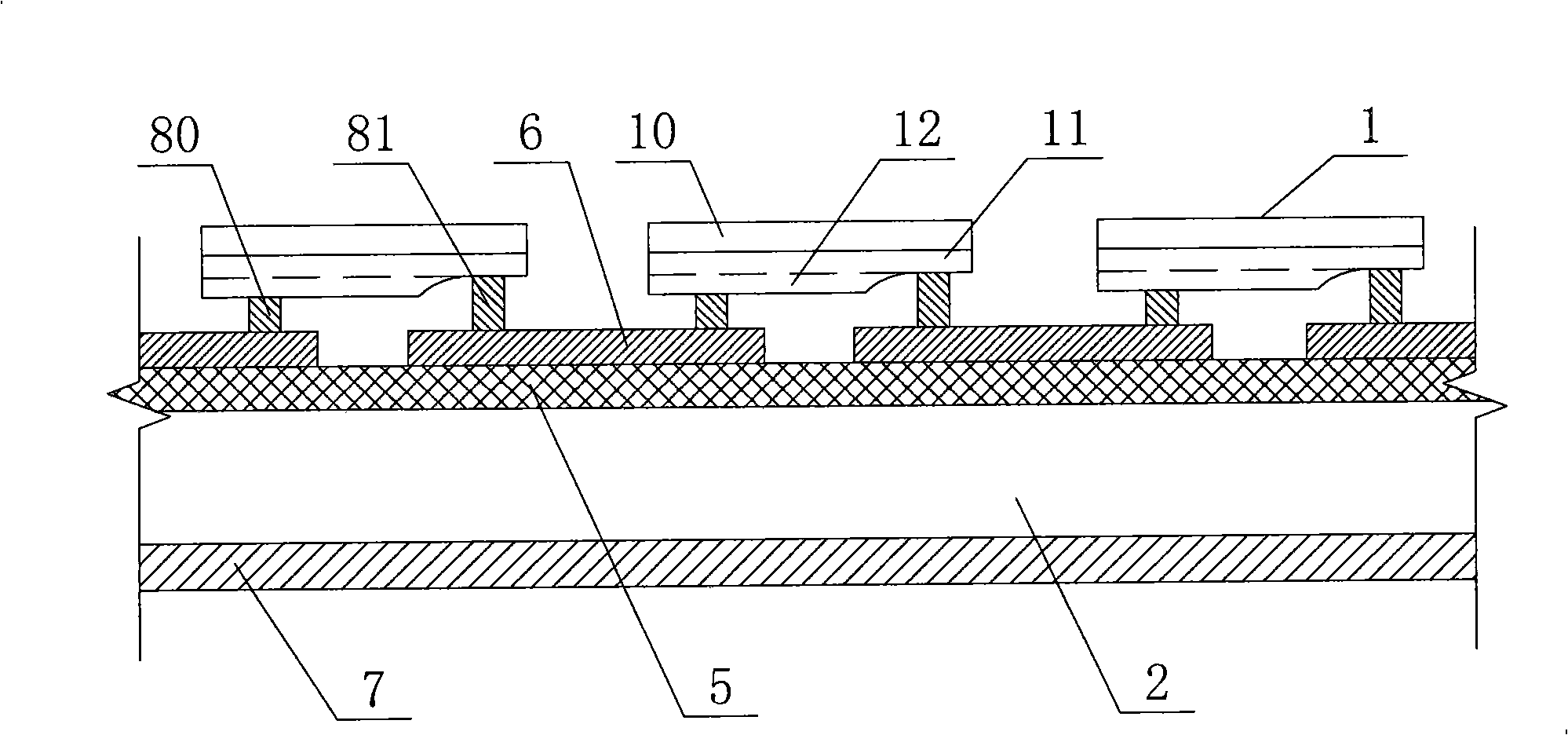
[0048] like figure 1 As shown, the high turn-on voltage flip-chip LED integrated chip of this embodiment includes several LED bare chips 1 and a silicon substrate 2, and the LED bare chips 1 include sapphire (Al 2 o 3 ) substrate 10 and gallium nitride (GaN) N-type epitaxial layer 11, P-type epitaxial layer 12, certainly, described substrate 10 also can be the substrate of other materials such as silicon carbide (SiC), described silicon substrate 2 is a P-type silicon substrate, and a thermally conductive insulating layer II 5 is deposited on the silicon substrate 2. The thermally conductive insulating layer II 5 is composed of a silicon nitride layer. The thermal conductivity of silicon nitride is very high, and its thermal conductivity is higher than that of Generally, the heat-conducting adhesive is more than 100 times higher, and the thickness of the heat-conducting insulating layer II 5 is thin, so the thermal conductivity is good, and it can play a good role in heat con...

Embodiment 2

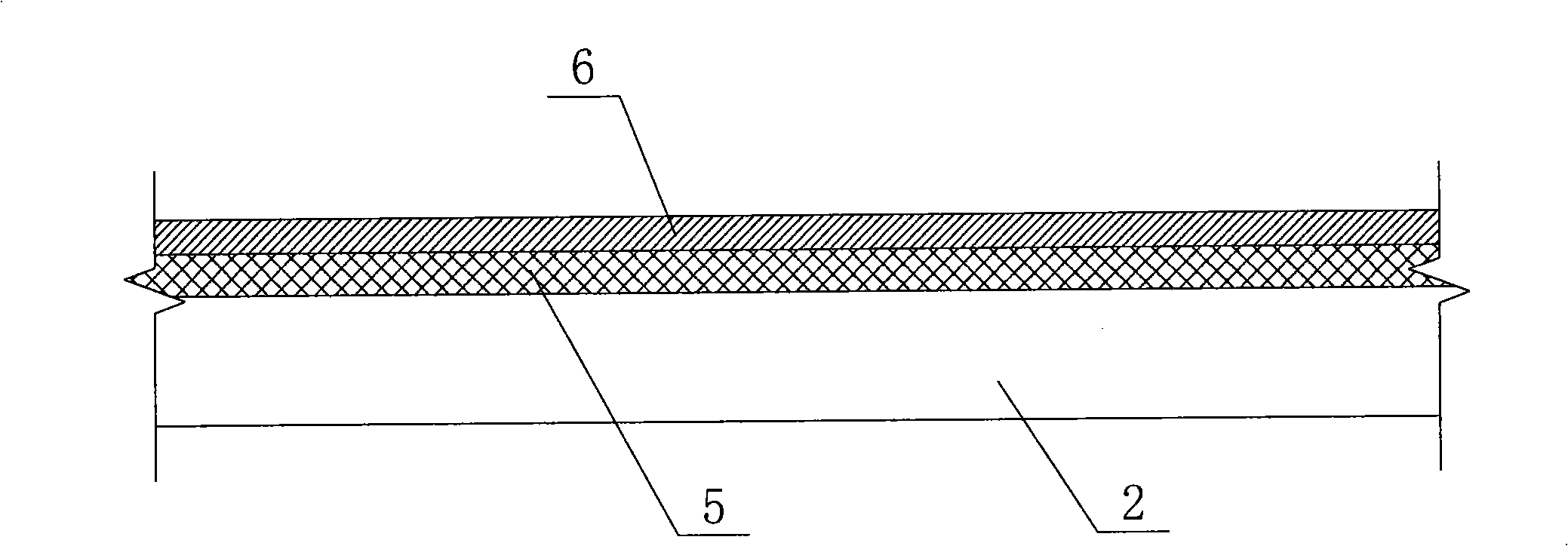
[0060] like Image 6 As shown, the high turn-on voltage flip-chip LED integrated chip of this embodiment includes several LED bare chips 1 and a silicon substrate 2, and the LED bare chips 1 include sapphire (Al 2 o 3) substrate 10 and gallium nitride (GaN) N-type epitaxial layer 11, P-type epitaxial layer 12, certainly, described substrate 10 also can be the substrate of other materials such as silicon carbide (SiC), described silicon substrate 2 is a P-type silicon substrate, and a layer of N+ diffusion layer 3 is diffused inwardly on the front side of the silicon substrate 2, and a layer of thermally conductive insulating layer I4 is grown on the N+ diffused layer 3, and on the thermally conductive insulating layer I4 A thermally conductive insulating layer II5 is formed, the thermally conductive insulating layer I4 is composed of silicon dioxide, and the thermally conductive insulating layer II5 is composed of silicon nitride. The thermal conductivity of silicon dioxide a...


PUM


Abstract

The invention discloses a high break-over voltage LED flip-chip and the fabrication method thereof, which is easy to integrate, low in cost, good in heat dissipation effect and good in high voltage resistance. The integrated chip comprises a plurality of LED flip-chips(1) and a plurality of silicon bulks(2); each LED flip-chip(1)is composed of an underlay(10), an N type epitaxial layer(11) and a P type epitaxial layer(12); at least one heat conduction insulated layer is developed on each silicon bulk(2); metal layers(6) are deposited on the heat conduction insulated layers; the corresponding N type epitaxial layers(11) and P type epitaxial layers(12) of the LED flip-chips(1) are reversely welded respectively on two separate metal layers through weld beads(80,81). The LED flip-chips (1) are connected into a circuit through the metal layers (6). The fabrication method includes the steps of forming the heat conducting insulated layer, the metal layers and an LED flip-chip enclosure.

Description

technical field [0001] The invention relates to a flip-chip LED integrated chip with high conduction voltage; in addition, the invention also relates to a manufacturing method of the flip-chip LED integrated chip with high conduction voltage. Background technique [0002] Flip-chip technology is one of the most advanced microelectronic packaging technologies today. It is not only a chip interconnection technology, but also an ideal chip bonding technology, which raises the circuit assembly density to a new level. Among all surface mount technologies, flip chip can achieve the smallest and thinnest package. As the size of electronic products shrinks further, the application of flip chip will become more and more extensive. The packaging form in which the LED bare chip is buckled upside down on the substrate is called a flip-chip LED. The traditional flip-chip LED uses a large power LED chip with high cost. Due to the large chip area and concentrated heat source, the heat dis...

Claims


Application Information

Patent Timeline
Patent Type & Authority Applications(China)
IPC IPC(8): H01L25/00H01L25/075H01L23/367H01L21/60
CPCH01L2224/16225
Inventor 吴纬国
Owner NANKER GUANGZHOU SEMICON MFG
Why Eureka
Try Eureka