

Novel wideband microband coupler based on defect place structure
A defect structure and coupler technology, applied in waveguide devices, electrical components, connecting devices, etc., can solve problems such as narrow bandwidth, achieve low resonance frequency, wide operating bandwidth, and improve the effect of coupling mode impedance
- Summary
- Abstract
- Description
- Claims
- Application Information
AI Technical Summary
Problems solved by technology
Method used
Image

Examples
specific Embodiment
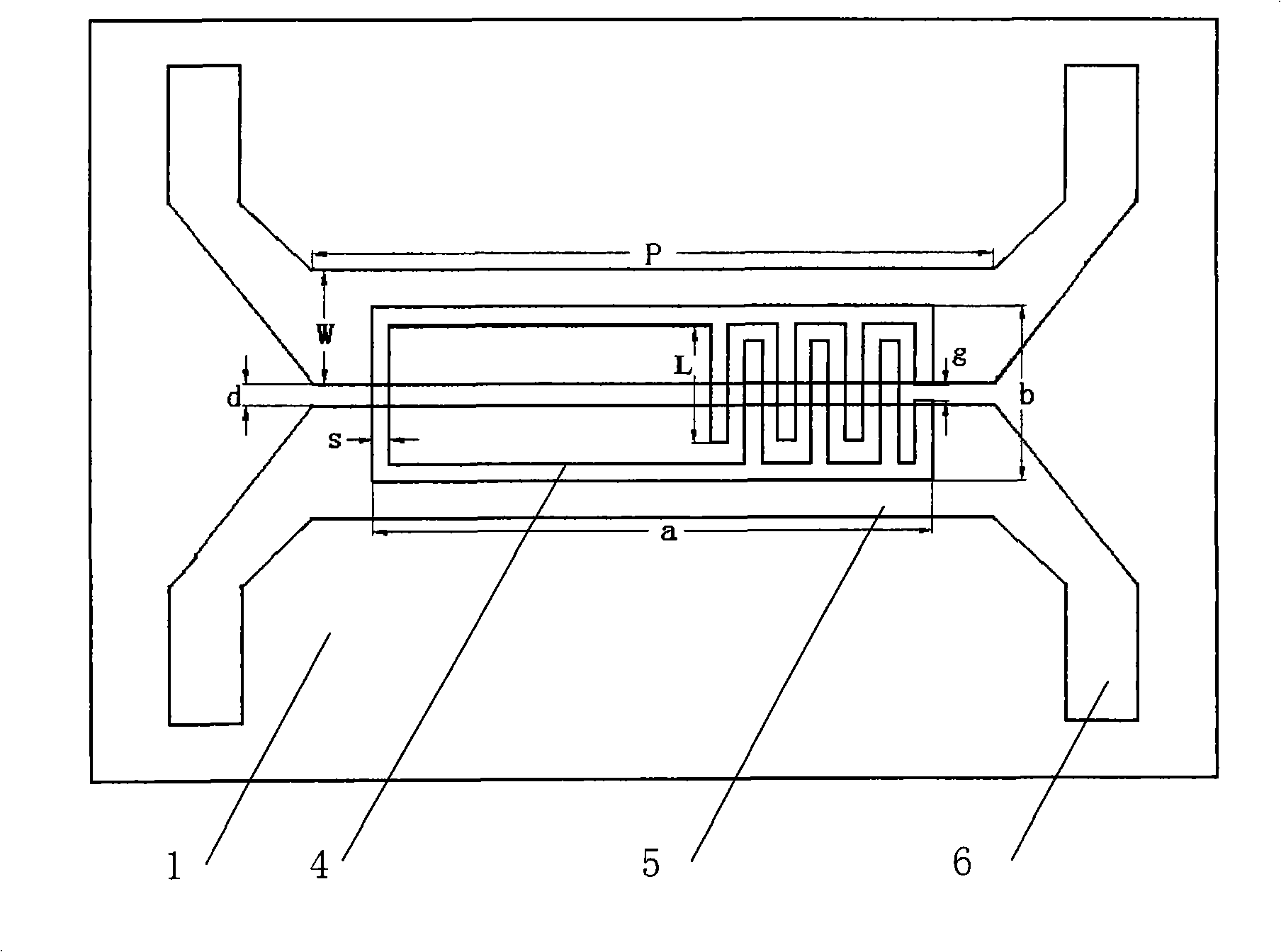
[0030] Such as figure 1 The schematic diagram of the structure of the novel broadband coupling microstrip directional coupler based on the defective ground structure includes: ground layer 1 defective ground structure 4 and microstrip structure signal layer 5; specific examples are as follows:
[0031] The signal layer 5 with two microstrip structures has a distance d between the inside of the long side P of the two signal layers 5 with a microstrip structure. There are two ports 6 at both ends of the signal layer 5 of each microstrip structure.
[0032] The defective ground structure 4 is placed symmetrically to the spacing d, and the opening g of the defective ground structure 4 is placed coincident with the spacing d of the signal layer 5 of the microstrip structure.
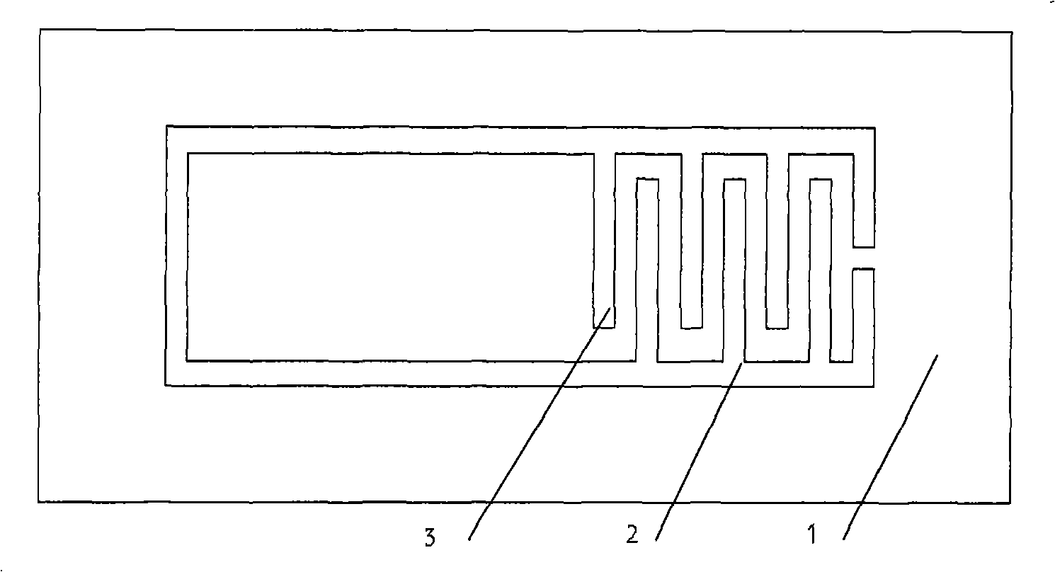
[0033] Such as figure 2 Schematic diagram of a defective ground structure in the shape of a split ring loaded with interdigitated lines. The defective ground structure 4 is composed of a ground layer 1, a ...
PUM
| Property | Measurement | Unit |
|---|---|---|
| Reflection coefficient | aaaaa | aaaaa |
| Isolation | aaaaa | aaaaa |
Abstract
Description
Claims
Application Information