Multi-layer printed circuit board, design method thereof, and final product of mainboard

A technology of multi-layer printing and design method, which is applied in the direction of multi-layer circuit manufacturing, printed circuit components, printed circuits connected with non-printed electrical components, etc. and other problems, to achieve the effect of improving interconnection density and saving space.

Active Publication Date: 2008-11-19
HUAWEI DEVICE CO LTD
View PDF0 Cites 12 Cited by
  • Summary
  • Abstract
  • Description
  • Claims
  • Application Information

AI Technical Summary

Problems solved by technology

[0008] In the process of implementing the present invention, the inventor found that the prior art has at least the following problems: in the HDI design of high-density radio frequency single board, when the signal

Method used


Image

  • Multi-layer printed circuit board, design method thereof, and final product of mainboard
  • Multi-layer printed circuit board, design method thereof, and final product of mainboard
  • Multi-layer printed circuit board, design method thereof, and final product of mainboard

Examples


Embodiment Construction

[0038] The embodiment of the present invention aims to provide a design method for a multilayer printed circuit board, a main board of an end product, and a multilayer printed circuit board that can save the space occupied by via holes and increase the interconnection density. Detailed description.

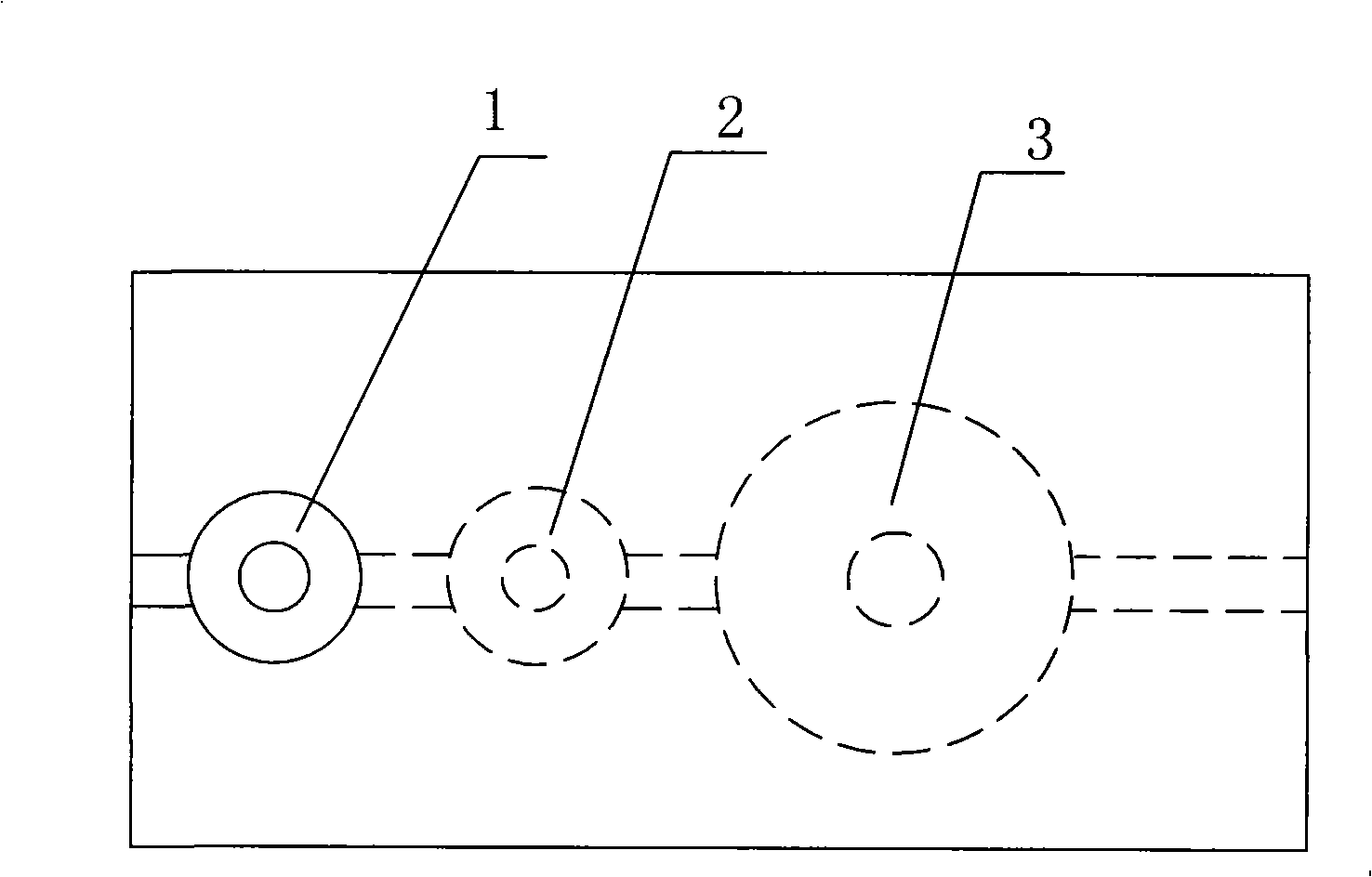
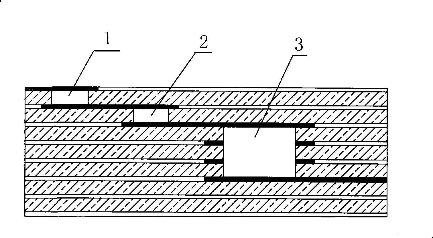
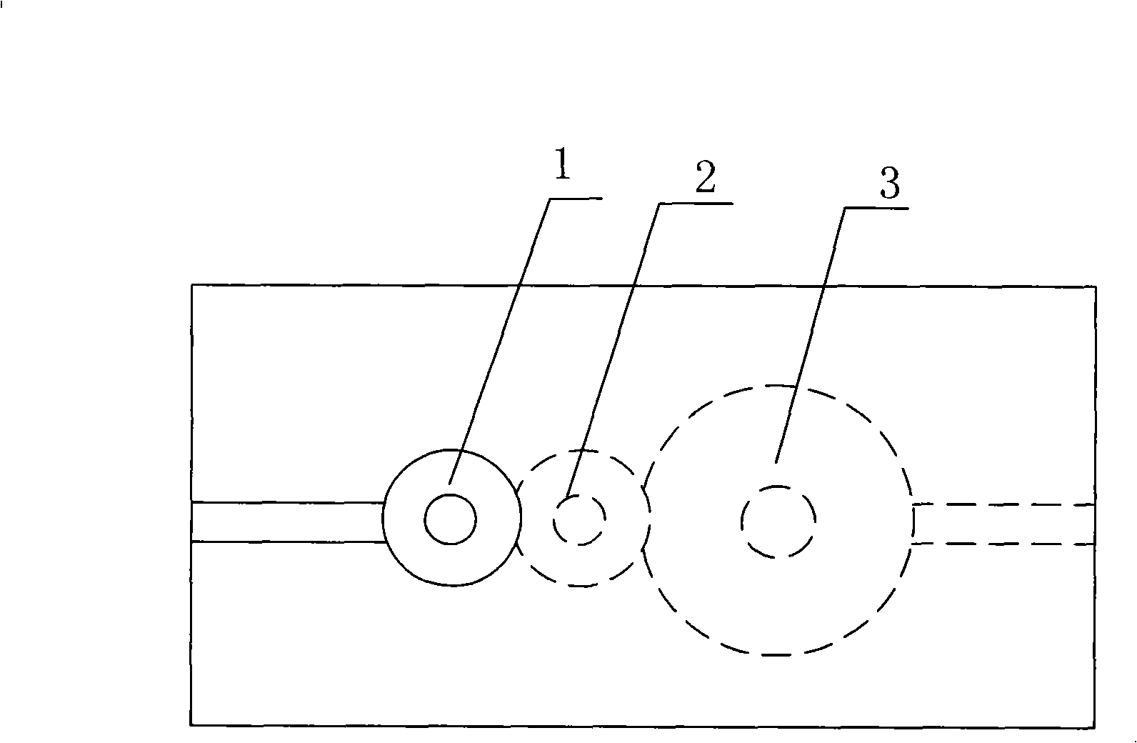
[0039] refer to image 3 , Figure 4 As shown, the multilayer printed circuit board of the embodiment of the present invention includes a substrate 100, on which a conductor circuit layer 101 and an interlayer insulating layer 102 are repeatedly formed in an alternating manner on the substrate 100; the conductor in this embodiment The circuit layer 101 has eight layers, and the interlayer insulating layer 102 has seven layers. In the interlayer insulating layer 102, a signal connection via hole is provided. The signal connection via hole in this embodiment includes a microhole 1 from the first layer to the second layer, and a microhole from the second layer to the third layer. ...


PUM


Abstract

The invention discloses a multi-layered printed circuit board and a design method thereof and a terminal product motherboard, which are invented for solving the problems that the space occupied by through holes can be saved, and the interconnection density can be improved. In the multilayered printed circuit board, the terminal pad center distance of the signal communication through holes between two different interlamination insulating layers at the position of replacing layers is larger than the terminal pad radius of any one of the signal communication through holes thereof, and less than the sum of the terminal pad radius of the two signal communication through holes. The terminal product motherboard adopts the multilayered printed circuit board; the design method of the multilayered printed circuit board comprises the steps that the terminal pad center distance of the two adjacent signal communication through holes is punched in a simulation model, the terminal pad center distance is larger than any one of the terminal pad radius thereof, and less than the replaced layer signal communication through hole of the sum of the terminal pad radius of the two signal communication through holes. The embodiment of the invention is applied in the manufacture and the design of the multilayered printed circuit board.

Description

technical field [0001] The invention relates to the field of integrated electronics, in particular to a multilayer printed circuit board and a design method thereof. Background technique [0002] The requirements for miniaturization, light weight and low cost of modern electronic devices are constantly increasing, which promotes the rapid development of microelectronic integration technology, and various new technologies such as high density interconnection HDI (High Density Interconnection) continue to emerge. [0003] High-density interconnection HDI substrate is defined as a substrate with a higher connection density per unit area than a general printed circuit board PCB (Printed CircuitBoard). Compared with ordinary PCBs, the line width and line spacing of high-density interconnect HDI substrates are finer. [0004] Using a multilayer interconnection design can reduce the area of ​​the printed circuit board. A multilayer printed circuit board is a multilayer structure ...

Claims


Application Information

Patent Timeline
IPC IPC(8): H05K3/46H05K1/11H05K1/18G06F17/50
Inventor 刘秀兰
Owner HUAWEI DEVICE CO LTD
Why Eureka
Try Eureka