Image sensor chip scale package having inter-adhesion with gap and method of the same

A die and tool technology, applied in the field of diffusion type wafer-level packaging, can solve the problems of difficulty in saving manufacturing costs and difficulty in reaching the same level of die surface, and achieves a simple method, easy control of panel thickness, and simple manufacturing procedures. Effect

Inactive Publication Date: 2008-11-26
ADVANCED CHIP ENG TECH INC
View PDF1 Cites 7 Cited by
  • Summary
  • Abstract
  • Description
  • Claims
  • Application Information

AI Technical Summary

Problems solved by technology

Since it needs to heat-cure the mold material, it may lead to warpage, making it difficult to achieve the same level of grain surface and mold material, and it is necessary to grind the uneven surface by chemical mechanical polishing, so it is also difficult to save manufacturing costs.

Method used


Image

  • Image sensor chip scale package having inter-adhesion with gap and method of the same
  • Image sensor chip scale package having inter-adhesion with gap and method of the same
  • Image sensor chip scale package having inter-adhesion with gap and method of the same

Examples


Embodiment Construction

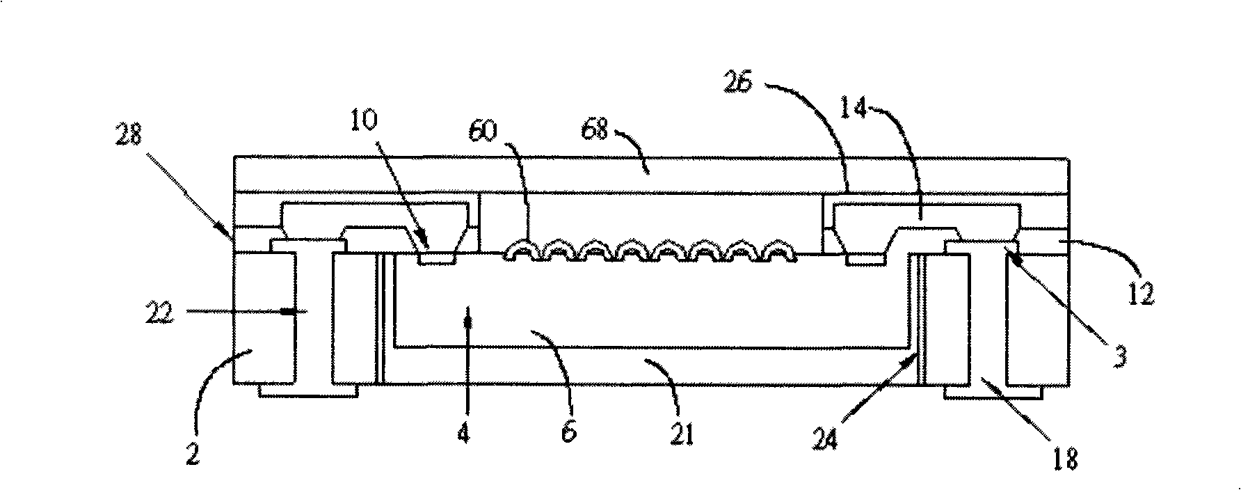
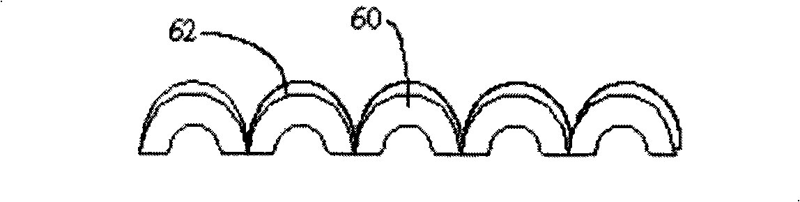
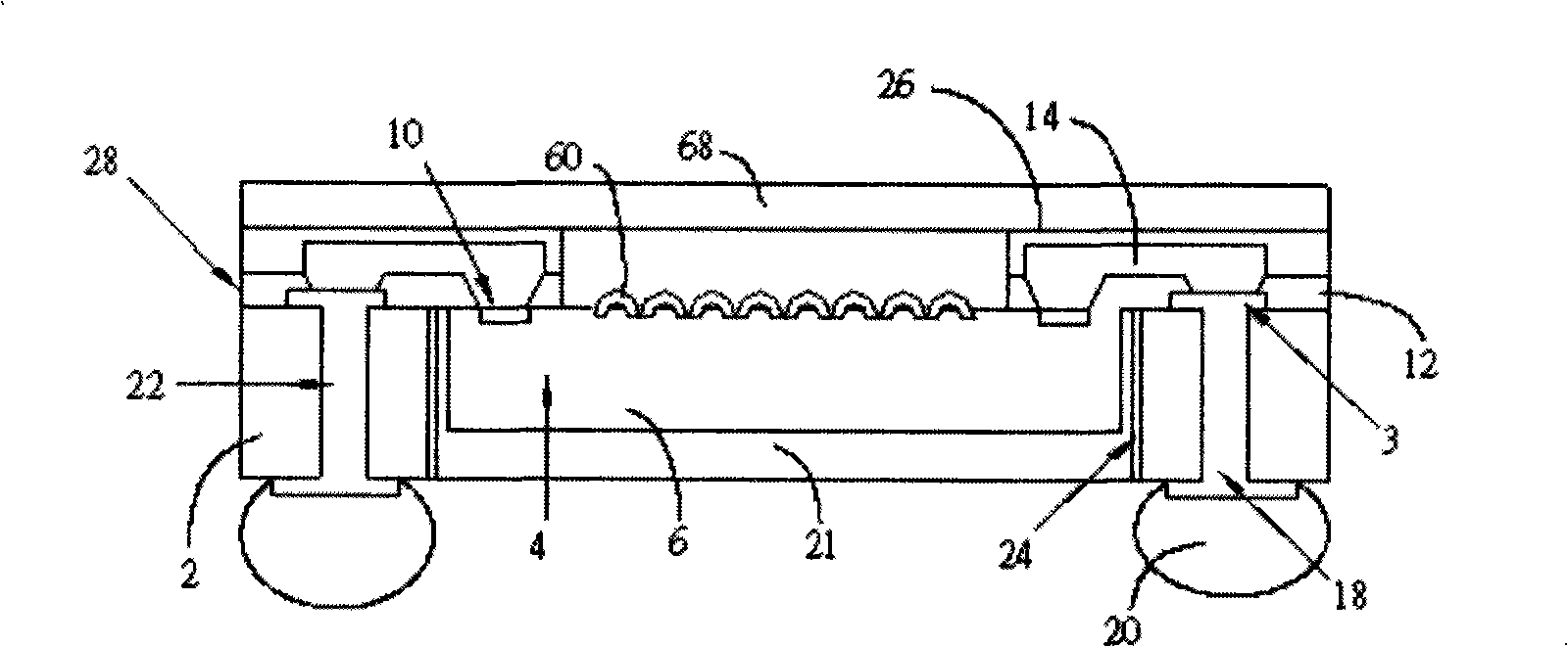
[0028] Certain similar embodiments of the invention will not be described in detail. However, it should be understood that all the preferred embodiments in the present invention are only used for illustration rather than limitation. Therefore, except for the preferred embodiments herein, the present invention can also be widely applied in other embodiments. The dimensions of different components are not particularly described, and the dimensions of some related components are enlarged and meaningless parts are omitted to make the description clear and emphasize the content of the present invention.

[0029] The present invention discloses a diffused WLP using a substrate 2 with a predetermined terminal metal contact pad 3 and a die receiving through hole 4 formed thereon. The die is disposed in the die-receiving via 4 of the substrate 2 and attached to a core paste, for example, an elastic core material filled between the edge of the die and the sidewall of the die-receiving v...


PUM

PropertyMeasurementUnit
thicknessaaaaaaaaaa
thicknessaaaaaaaaaa
elongationaaaaaaaaaa

Abstract

A packaging structure provided by the invention includes a substrate having a crystal grain receiving through hole, a contact through hole and a first contact pad; the crystal grains are placed in the crystal grain receiving through hole, wherein the crystal grains have a lenticule area. A transparent cover covers the lenticule area. Peripheral materials are formed below the crystal grains and fill a gap between the entering crystal grains and a side wall of the crystal grain receiving through hole. A dielectric layer is formed above the crystal grains and the substrate. A re-distribution layer is formed on the dielectric layer to couple the first contact pad. A protection layer is formed on the re-distribution layer. A second contact pad is formed on a lower surface of the substrate and below the contact through hole. And a transparent substrate is formed above the protection layer.

Description

technical field [0001] The present invention relates to a wafer level package (WLP) structure, and more particularly to a fan-out WLP with a substrate having die receiving vias and interconnect vias to improve reliability and reduce component size. Background technique [0002] The rapid development of semiconductor technology, and the trend of increasing semiconductor grain density and miniaturization. Therefore, such high-density packaging technology and interconnection technology are also improved to apply the above-mentioned conditions. In the traditional flip-chip structure, the array of solder balls is formed on the surface of the die, and the desired pattern is formed through the traditional solder paste and solder ball mask. Packaging functions include heat dissipation, signal transmission, power distribution, protection, etc. When chips become more complex, traditional packaging such as lead frame packaging, flexible packaging, and rigid packaging cannot meet the n...

Claims


Application Information

Patent Timeline
Patent Type & Authority Applications(China)
IPC IPC(8): H01L27/146H01L27/148H01L23/48H01L23/31H01L23/02H01L21/50H01L21/60H01L21/56H01L21/78
CPCH01L2924/14H01L2924/15311H01L24/13H01L27/14643H01L27/14618H01L27/14621H01L27/14627H01L27/14683H01L2924/19043H01L2924/10253H01L2924/01078H01L2924/01077H01L27/148H01L2924/01068H01L2924/01079H01L2224/05569H01L2224/05008H01L2224/05026H01L2224/05548H01L2224/05001H01L2224/05124H01L2224/05147H01L2224/05155H01L2224/05166H01L2224/05644H01L2224/05666H01L24/20H01L2224/02379H01L2924/00H01L2924/00014H01L2924/01029H01L2924/01028H01L2924/013H01L27/14
Inventor 杨文焜张瑞贤许献文林殿方
Owner ADVANCED CHIP ENG TECH INC
Why Eureka
Try Eureka