Optimization design method of micro-electron packaging device based on artificial neural network

A technology of artificial neural network and microelectronic packaging, applied in biological neural network models, instruments, calculations, etc.

Inactive Publication Date: 2008-12-10
GUILIN UNIV OF ELECTRONIC TECH
View PDF0 Cites 17 Cited by
  • Summary
  • Abstract
  • Description
  • Claims
  • Application Information

AI Technical Summary

Problems solved by technology

Traditional optimization methods, such as the orthogona

Method used


Image

  • Optimization design method of micro-electron packaging device based on artificial neural network
  • Optimization design method of micro-electron packaging device based on artificial neural network
  • Optimization design method of micro-electron packaging device based on artificial neural network

Examples


Embodiment Construction

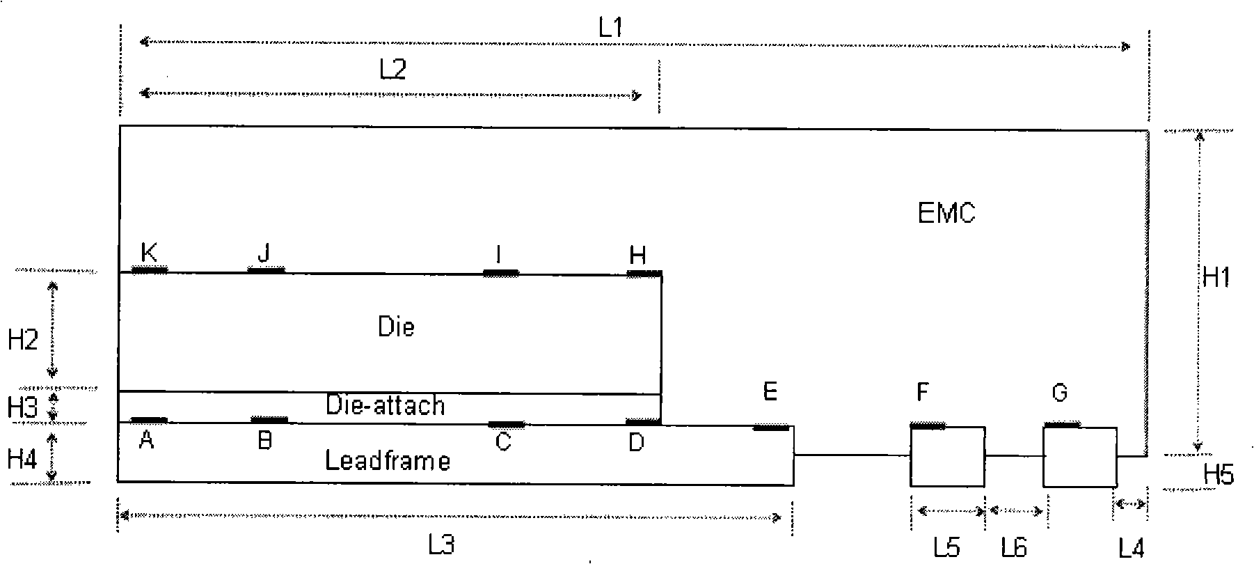
[0090] The user hopes to optimize the design of the QFN device according to the interface lamination failure between the silicon wafer adhesive DA and the lead-frame (lead-frame) under the comprehensive influence of humidity, heat and steam pressure as the design criterion. Such as image 3 shown. The loading process is: from the end of the package mold filling, after 186hr85℃HR85% pretreatment, then lead-free reflow soldering and cooling to -65℃.

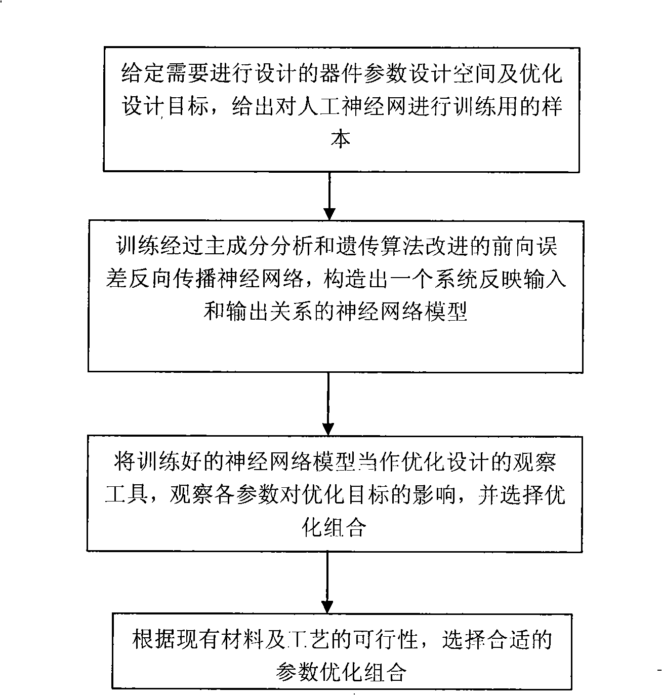
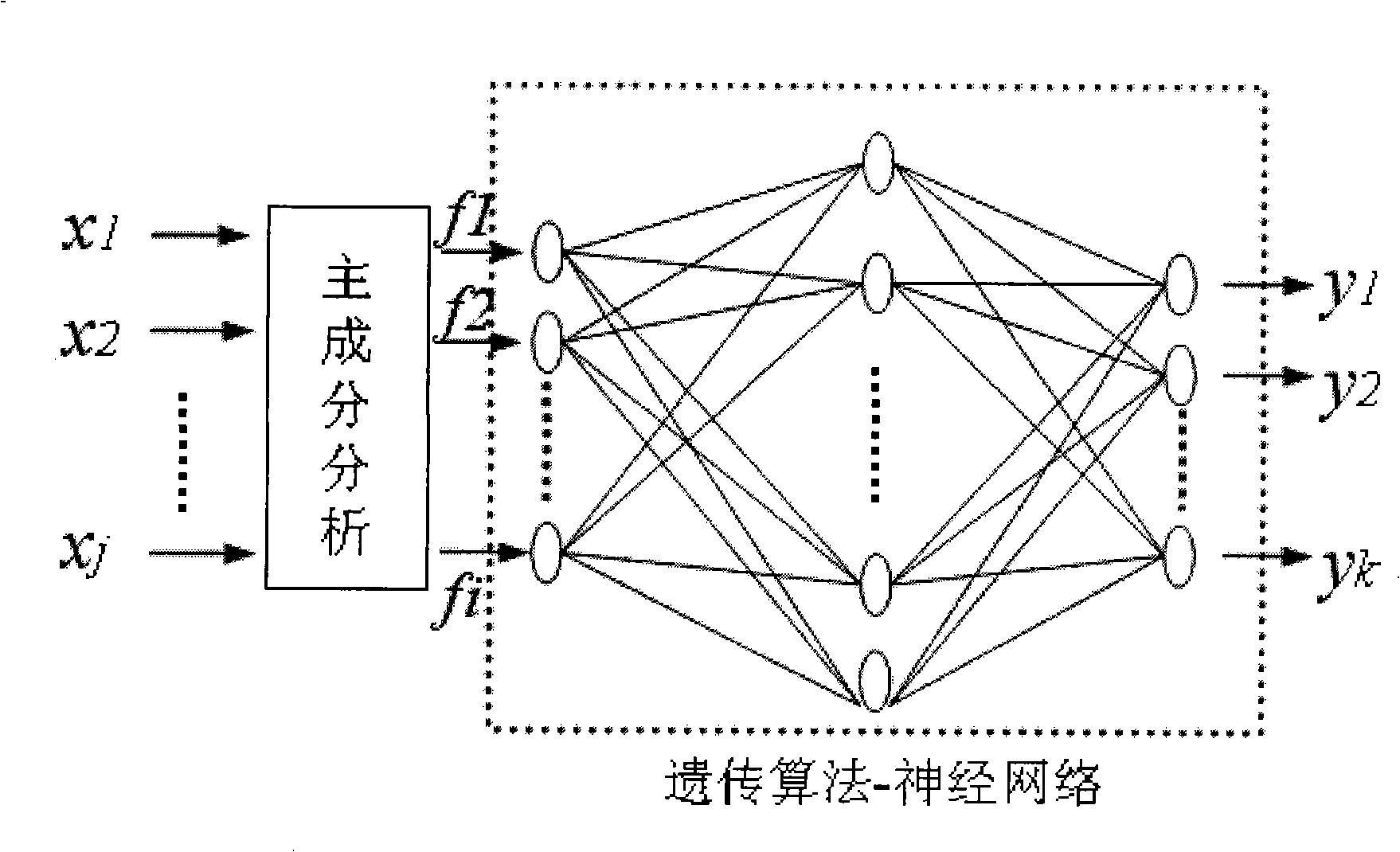
[0091] (1) The user specifies the device parameter design space to be designed and the optimization design goal, performs finite element analysis and analysis according to the uniform experiment method, and provides samples for training the artificial neural network.

[0092] (1.1) Designation of design parameters

[0093] The user specifies to optimize and select 6 material parameters of Young's modulus E (MPa) and thermal expansion coefficient α (ppm / ℃) of EMC, DA and lead-frame materials, and 6 structural parameters: the width...


PUM


Abstract

The present invention discloses an optimum design method of micro-electronic packaging device, based on an artificial neural network. The method comprises the following steps: (1) the user provides the parameter design space and the optimum design objective of the device to be designed, and the sample used for training the artificial neural network; (2) the training adopts a neural network of forward error and converse transmission, which is improved by main component analysis and genetic algorithm, and constructs a neural network model with a system reflecting the relation between the input and the output; (3) the trained neural network model is used as an observation tool of optimum design for observing the influence of the parameters on the optimum objective and selecting the optimum combination; (4) the proper optimum combination of the parameters is selected according to the feasibility of materials and technologies. The optimum design method solves the design problem of reliability of material collocation and size collocation, suits the optimum design of different types of packaging devices, and can be applied to the field of optimum design of various categories of multi-objective or multi-factor complex systems.

Description

technical field [0001] The invention relates to the technical field of microelectronic packaging, in particular to an optimal design method of a microelectronic packaging device based on an artificial neural network. Background technique [0002] The reliability optimization design of microelectronic packaging devices is an important aspect in the field of packaging manufacturing. Because the reliability of actual packaged devices is affected by various factors, the failure mechanism is a complex nonlinear relationship, such as material properties, structural parameters, environmental parameters, process parameters, and so on. Therefore, in order to optimize the design through reliability, it is an indispensable link to optimize the selection of various parameters of the device for a key failure mechanism of the packaged device, and to improve the reliability of the microelectronic packaged device. Moreover, most of the current optimal design methods for packaged devices ar...

Claims


Application Information

Patent Timeline
IPC IPC(8): G06F17/50G06N3/06
Inventor 杨道国蔡苗
Owner GUILIN UNIV OF ELECTRONIC TECH
Why Eureka
Try Eureka