

Method for preparing ALON protection film for optical element
A technology for optical components and protective films, applied in the field of preparation of AlON protective films for optical components, can solve the problems of opaque application range, large absorption, and large stress in the visible light band, and achieve high transmittance, low absorption coefficient, and mechanical strength. high effect
- Summary
- Abstract
- Description
- Claims
- Application Information
AI Technical Summary
Problems solved by technology
Method used
Image

Examples
Embodiment 1
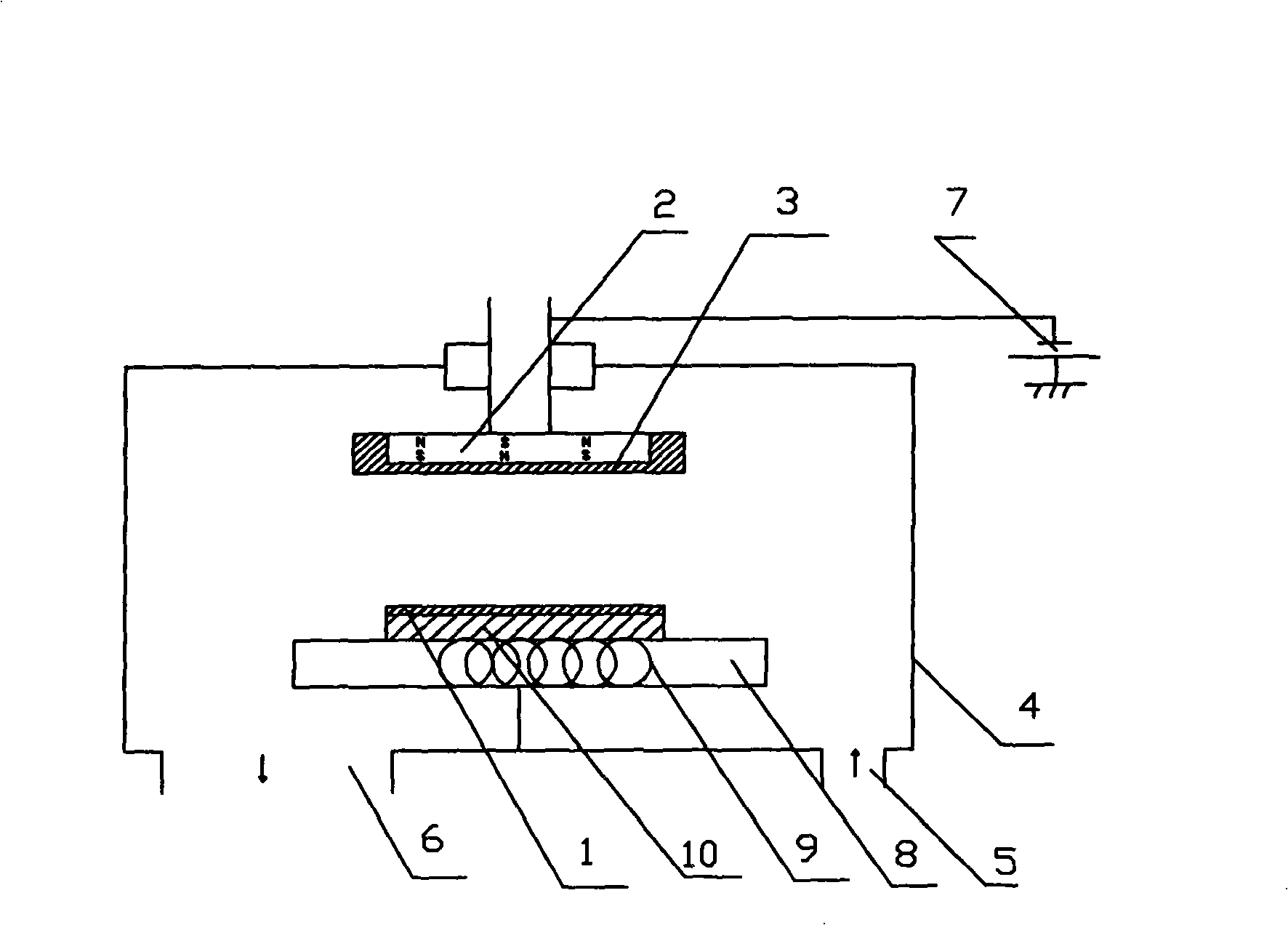
[0023] (1) Install the equipment according to the above steps, the optical element substrate 10 is placed on the substrate stage 8, the material of the optical element substrate 10 is KCl, and the vacuum chamber 4 is first vacuumed to be higher than 3 * 10 -3 Pa, then adopt resistive heating mode, the optical element substrate 10 is heated to 200C;
[0024] (2) Fill the vacuum chamber 4 with Ar gas, keep the vacuum at 0.2Pa, adopt the radio frequency magnetron sputtering process, sputtering power 300W, and bombard and clean the surface of the Al target 3 for 10 minutes;
[0025] (3) Press N 2 / (N 2 +O 2 )=0.5, (N 2 +O 2 ) / Ar=0.2 ratio into Ar, N 2 Gas and O 2 Gas mixed gas, working vacuum 0.2Pa, adopt radio frequency magnetron sputtering process, keep sputtering power 100W, control deposition rate and deposition time, plate 100nm thick plate type AlON protective film 1 on both sides of optical substrate 10;
[0026] (4) After the deposition is completed, the temperature...
Embodiment 2
[0030] (1) Install the equipment according to the above steps, the optical element substrate 10 is placed on the substrate table 8, the material of the optical element substrate 10 is ZnSe, first the vacuum chamber 4 is evacuated to be higher than 3 * 10 -3 Pa, then adopt resistance heating mode, the optical element substrate 10 is heated to 500C;
[0031] (2) Fill the vacuum chamber 4 with Ar gas, keep the vacuum at 0.3Pa, adopt the radio frequency magnetron sputtering process, sputtering power 100W, and bombard and clean the surface of the Al target 3 for 10 minutes;
[0032] (3) Press N 2 / (N 2 +O 2 )=0.6, (N 2 +O 2 ) / Ar=0.2 ratio into Ar, N 2 Gas and O 2 Gas mixed gas, working vacuum 0.2Pa, adopt radio frequency magnetron sputtering process, keep sputtering power 200W, control deposition rate and deposition time, coat 800nm thick spherical crown type AlON protective film 1 on both sides of optical substrate 10;
[0033] (4) After the deposition is completed, the t...
Embodiment 3
[0037] (1) Install the equipment according to the above steps, the optical element substrate 10 is placed on the substrate table 8, the material of the optical element substrate 10 is Ge, and the vacuum chamber 4 is first vacuumed to be higher than 3 × 10 -3 Pa, then adopt resistive heating mode, the optical element substrate 10 is heated to 400C;
[0038] (2) Fill the vacuum chamber 4 with Ar gas, keep the vacuum at 0.1Pa, adopt DC magnetron sputtering process, sputtering power 500W, and bombard and clean the surface of the Al target 3 for 8 minutes;
[0039] (3) Press N 2 / (N 2 +O 2 )=0.2, (N 2 +O 2 ) / Ar=0.3 ratio into Ar, N 2 Gas and O 2 Gas mixed gas, working vacuum 0.2Pa, adopting DC magnetron sputtering process, keeping sputtering power 50W, controlling deposition rate and deposition time, coating 80nm thick flat AlON protective film 1 on both sides of optical substrate 10;
[0040](4) After the deposition is completed, the temperature of the workpiece is slowly l...
PUM
| Property | Measurement | Unit |
|---|---|---|
| Microhardness | aaaaa | aaaaa |
| Microhardness | aaaaa | aaaaa |
| Hardness | aaaaa | aaaaa |
Abstract
Description
Claims
Application Information