
Method for preparing crystal round back electrode and crystal round

A back electrode and wafer technology, applied in the manufacturing of circuits, electrical components, semiconductor/solid-state devices, etc., can solve the problems of unstable dispensing product qualification rate, lower output per unit time, and low glue fluidity, etc., to eliminate Flanging phenomenon, saving storage costs, improving the effect of quality control

Inactive Publication Date: 2009-01-21
GUANGDONG FENGHUA ADVANCED TECH HLDG +1
View PDF0 Cites 13 Cited by
  • Summary
  • Abstract
  • Description
  • Claims
  • Application Information

AI Technical Summary

Problems solved by technology

Since the conductive adhesive and the base are connected together, chain reactions are likely to occur during the packaging process, that is, the quality of the connection between the conductive adhesive and the base will directly affect the final electrical performance of the product, which will lead to poor pass rate of dispensing products. Stable; on the other hand, compared with the eutectic chip bonding method adopted by the diode and triode, the production speed will be much slower and the output per unit time will be reduced, which is to improve production efficiency and reduce production A technical bottleneck of cost; and the fluidity of the glue is low, and the edge phenomenon is unavoidable

Method used


Image

  • Method for preparing crystal round back electrode and crystal round
  • Method for preparing crystal round back electrode and crystal round
  • Method for preparing crystal round back electrode and crystal round

Examples


Embodiment Construction

[0021] (1) Prepare the wafer and keep the wafer flat during the whole preparation process: use a porous ceramic plate to support the wafer, obtain a vacuum through the channels of the porous ceramic on the plate, suck the wafer firmly without damage and keep the wafer in the subsequent steps remain flat in

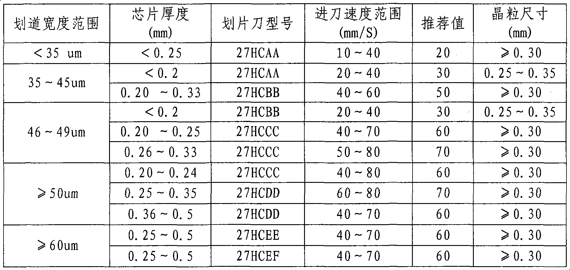
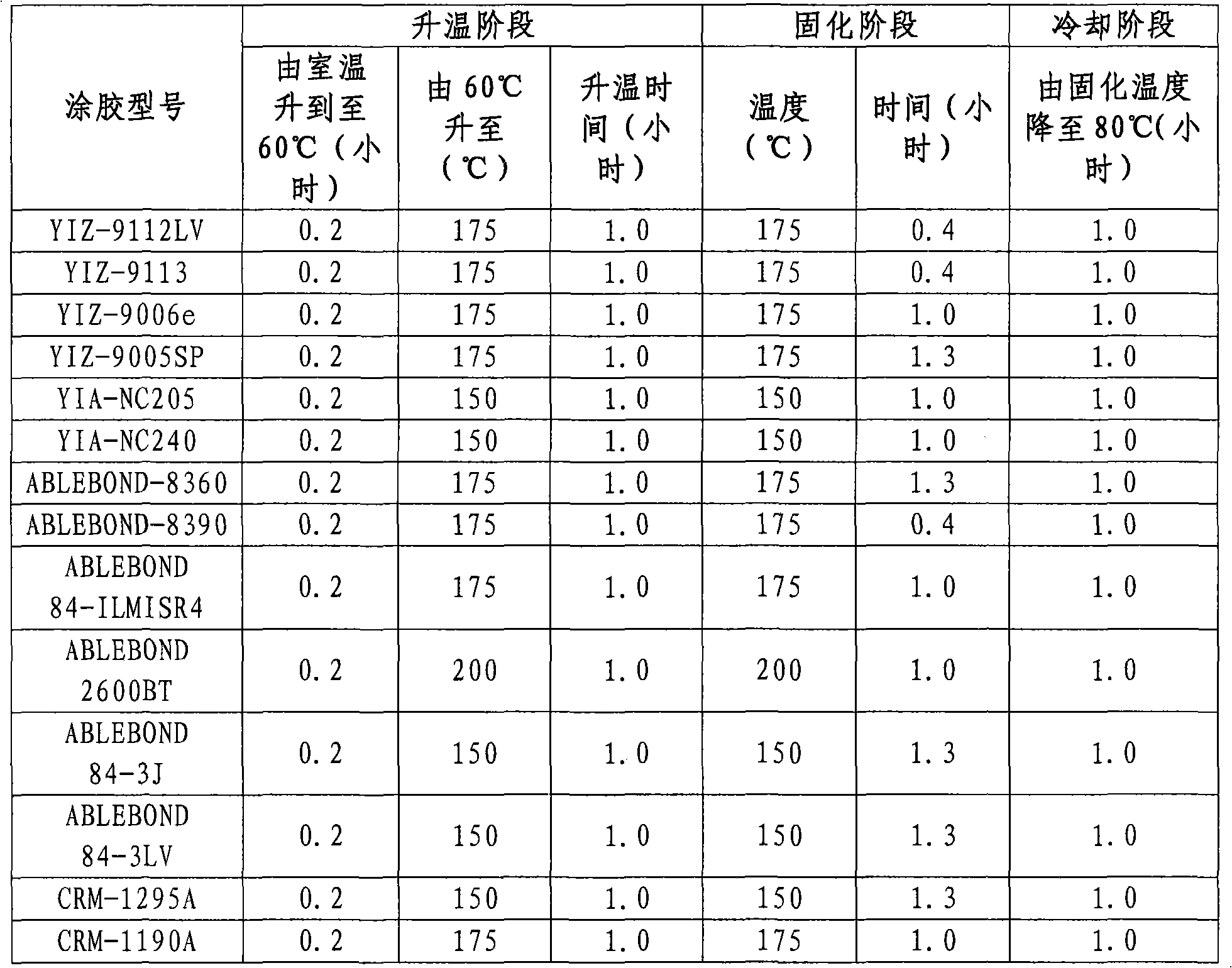
[0022] Paste the adhesive film and metal ring on the wafer, and mark the production batch number and product model on the adhesive film. Since the wafer is adsorbed on the surface of the workbench during printing, if the surface is uneven, uneven coating will occur when the adhesive is applied on the back of the next step, which indirectly leads to insufficient dispensing amount and affects product packaging. post pass rate. Therefore, the flatness of the workbench is not greater than 0.025mm; the repeated positioning accuracy of the workbench can only meet the process requirements when it reaches 0.1mm; because the parallelism between the screen and the workbench during ...


PUM


Abstract

The invention discloses a wafer whose back side is coated with adhesive through adopting the silk screen printing and a process for preparing a back electrode of the wafer, the preparation process comprises the following five steps: preparing a wafer, and keeping the wafer flat in the subsequent steps, adopting the silk screen printing to coat the adhesive on the back side of the wafer and drying, arranging the wafer which is coated with the adhesive on a scribing blue film, separating, adhering and solidifying the separated wafer. The process eliminates the flanging phenomenon which easily occurs during the preparation of the wafer, the dosage of bonding slurry is reduced by one-third, the cost of the bonding slurry is greatly reduced by about ten percent, and the flatness of the coating surface of a back electrode of the chip is guaranteed, a scribing is easily cut, the intensity of the combination between the chip and the electrode during the eutectic welding is guaranteed, and the production time and cost are greatly saved. The wafer whose back side is coated with the adhesive of the invention can be stored for a long time, and the control to the quality of the stock is improved.

Description

technical field [0001] The invention relates to a manufacturing method of a wafer back electrode and a wafer thereof, in particular to a method for coating adhesive on the back of the wafer by screen printing. Background technique [0002] Wafer refers to the silicon wafer used in the manufacture of silicon semiconductor integrated circuits. Because of its circular shape, it is called a wafer. It can be processed into various circuit element structures on silicon wafers, and become IC products with specific electrical functions. With the rapid development of electronic products, wafers are widely used to make FH431 voltage reference power supply and power MOS devices, etc., mainly used in computer motherboards, voltage monitors, voltage reference power supplies, switching power supplies (reference voltage), chargers and other consumption electronics field. FH431 adjustable voltage reference power supply and power MOS devices have become important semiconductor power device...

Claims


Application Information

Patent Timeline
Patent Type & Authority Applications(China)
IPC IPC(8): H01L21/00H01L21/28
Inventor 胥小平戴春明张富启晏承亮沓世我赖小军黄海文
Owner GUANGDONG FENGHUA ADVANCED TECH HLDG
Learn More