

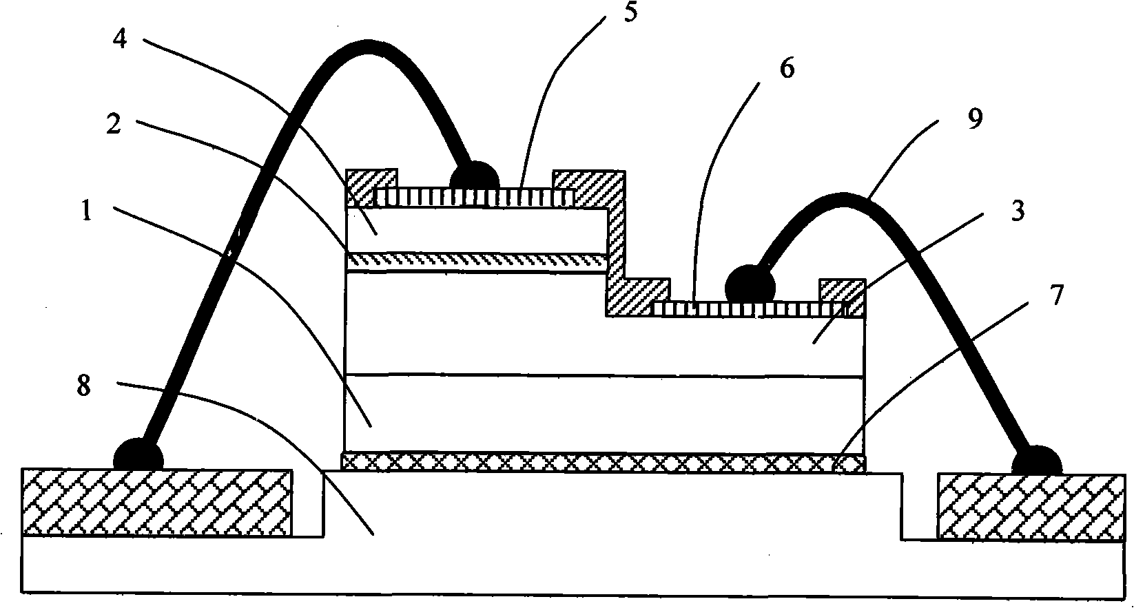
Salient point LED and manufacturing method thereof
A technology for light-emitting diodes and a manufacturing method, which is applied in the manufacturing of semiconductor/solid-state devices, electrical components, and electrical solid-state devices, etc., can solve the problems of lead occupied space, large package volume, restricting the application of multi-chip LED products, etc., and reduce the package size. The effect of relaxing the requirements of size and machining accuracy
- Summary
- Abstract
- Description
- Claims
- Application Information
AI Technical Summary
Problems solved by technology
Method used
Image

Examples
Embodiment 1
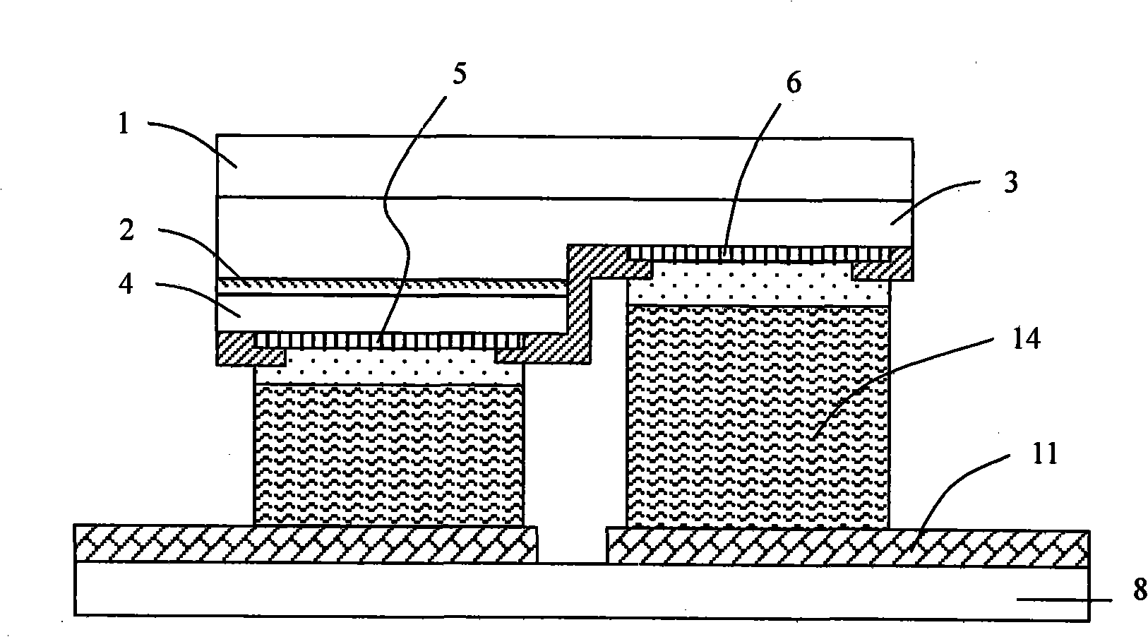
[0036] Combination of technologies, methods and designs adopted for the present invention Figure 5 For illustration, the drawings used are not drawn to scale. For the sake of simplicity, only one LED chip is used as an illustration, and LED chips of different sizes and wavelengths can be used in this embodiment. The manufacturing steps of the gold bump light-emitting diode chip are as follows:
[0037] 1. Form a passivation layer on the LED chip, such as Figure 5 As shown in 5-1;
[0038] 2. Sputtering titanium / gold is the metal sacrificial layer material to form the metal sacrificial layer 15, such as Figure 5 As shown in 5-2
[0039] 3. Make mask 16, such as Figure 5 As shown in 5-3;
[0040] 4. Make gold as the under-bump metal (UBM) material and fill the metal bump (Metal Bump / Stud) material 14 to form gold metal bumps, such as Figure 5 As shown in 5-4;
[0041] 5. Remove the mask 16, such as Figure 5 as shown in 5-5;
[0042] 6. Remove the metal sacrificial ...
Embodiment approach 2
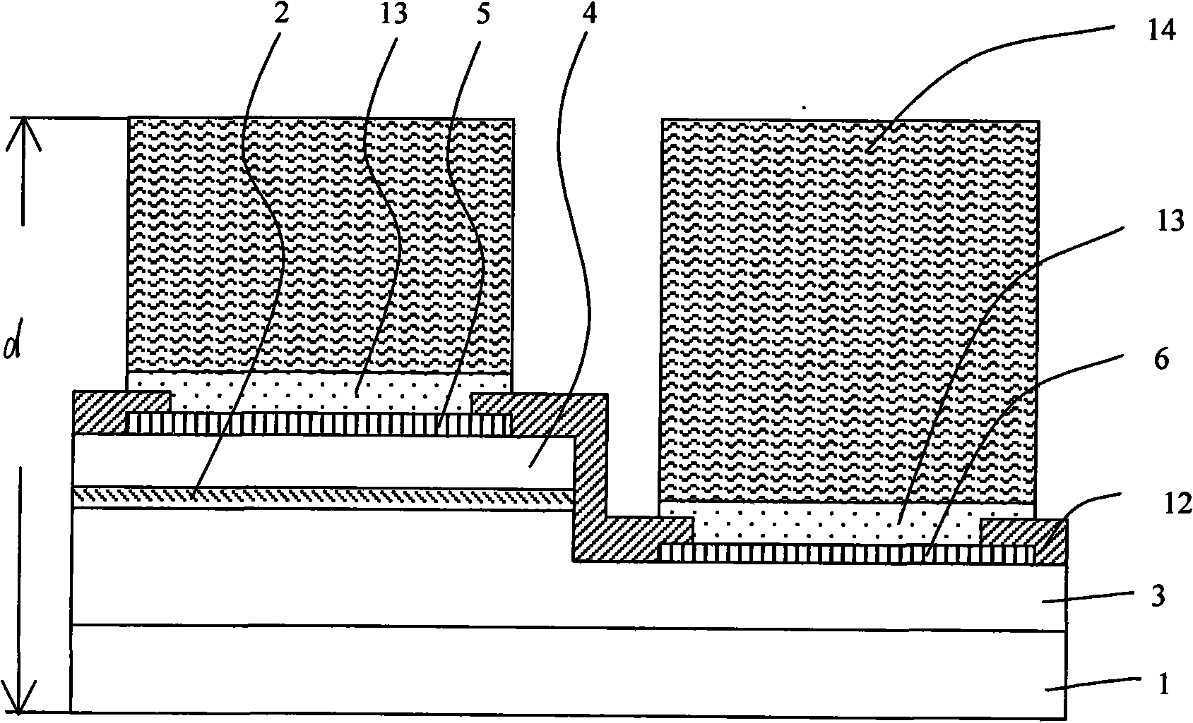
[0047] For the technology, method and design adopted in the present invention in conjunction with the attached Figure 6 Be explained. The drawings used are not drawn to scale. For the sake of simplicity, only one LED chip is used as an illustration, and LED chips of different sizes and wavelengths can be used in this embodiment. The manufacturing steps of the lead-tin alloy bump light-emitting diode chip are as follows:
[0048] 1. Form a passivation layer on the LED chip, such as Figure 6 As shown in 6-1;
[0049] 2. Sputter titanium / tungsten / copper alloy as the metal sacrificial layer material to form the metal sacrificial layer 15, such as Figure 6 As shown in 6-2;
[0050] 3, make photoresist mask 16, as Figure 6 As shown in 6-3;
[0051] 4. Copper electroplating is used as under-bump metal 13 (UBM) material and lead-tin alloy is electroplated as metal bump 14 (MetalBump / Stud) material to form lead-tin alloy metal bump 14, such as Figure 6 Shown in 6-4.
[00...
PUM
| Property | Measurement | Unit |
|---|---|---|
| thickness | aaaaa | aaaaa |
Abstract
Description
Claims
Application Information