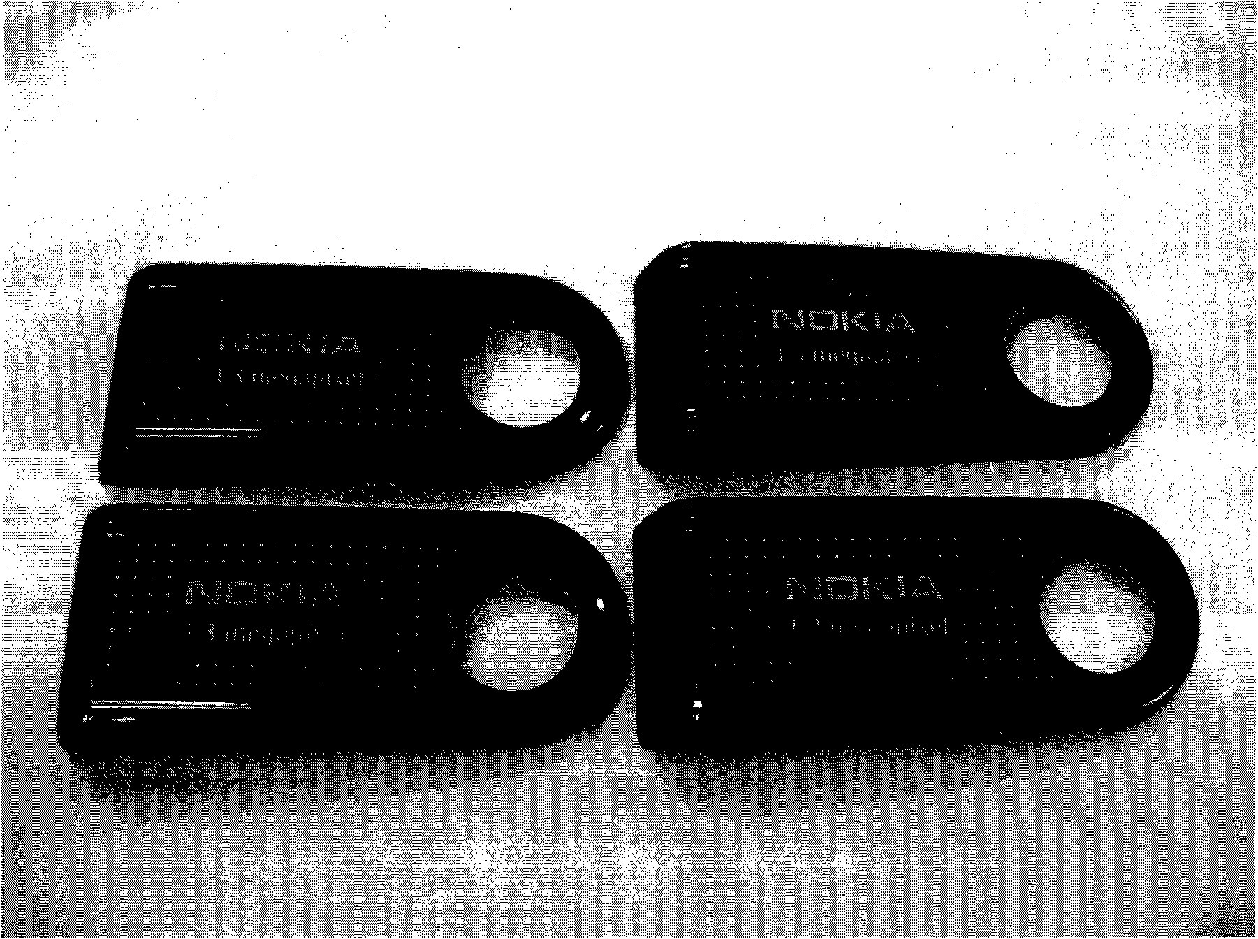
Outer casing of electronic product and preparation method thereof
A technology for electronic products and shells, which is applied in the field of electronic product shells and their preparation, and can solve the problem that the pattern of the shell does not have a metallic texture.
- Summary
- Abstract
- Description
- Claims
- Application Information
AI Technical Summary
Problems solved by technology
Method used
Image

Examples
preparation example Construction
[0012] The preparation method of the electronic product casing provided by the present invention comprises in turn forming a metal coating on the surface of the film layer; forming a printed pattern on the surface of the metal coating; removing the metal coating without a printed pattern on the surface, and then removing the printed pattern; The injection molding layer is formed on the top, so that the metal plating layer is located between the film layer and the injection molding layer.
[0013] The method of forming a metal coating on the surface of the film layer can be an electroplating method, an electroless plating method or a magnetron sputtering ion plating method, because the thickness of the sputtering coating obtained by the magnetron sputtering ion plating method is uniform and compared with the adhesion of the film layer Well, so it is preferred to use the magnetron sputtering ion plating method.
[0014] The magnetron sputtering ion plating method may be an exist...
Embodiment 1
[0033]Using magnetron sputtering ion plating equipment (multi-arc-magnetron sputtering ion coating machine, manufactured by Beijing Beiyi Innovation Vacuum Technology Co., Ltd., model JP-700), the PMMA sheet with a thickness of 0.175 mm is placed on the magnetic On the workpiece rack in the vacuum chamber of the controlled sputtering ion plating equipment, start the vacuum pump to evacuate, and the vacuum degree in the vacuum chamber reaches 4×10 -3 Pa, fill with argon to make the absolute pressure in the vacuum chamber 0.5 Pa, and adjust the temperature in the vacuum chamber to 150°C. Start the DC power supply (voltage is 400 volts, current is 15 volts) that is applied on the magnetron target (the target is 99.99% copper), and under the above-mentioned temperature and pressure conditions, sputter for 3 seconds, and the thickness is 0.175 mm A copper plating layer with a thickness of 10 micrometers was formed on the PC sheet.
[0034] On the screen printing machine, use Shenz...
PUM
| Property | Measurement | Unit |
|---|---|---|
| Thickness | aaaaa | aaaaa |
| Wavelength | aaaaa | aaaaa |
| Thickness | aaaaa | aaaaa |
Abstract
Description
Claims
Application Information
 - R&D
- Intellectual Property
- Life Sciences
- Materials
- Tech Scout
- Unparalleled Data Quality
- Higher Quality Content
- 60% Fewer Hallucinations
Browse by: Latest US Patents, China's latest patents, Technical Efficacy Thesaurus, Application Domain, Technology Topic, Popular Technical Reports.
© 2025 PatSnap. All rights reserved.Legal|Privacy policy|Modern Slavery Act Transparency Statement|Sitemap|About US| Contact US: help@patsnap.com