Method for eliminating probe needle track bias

A technology of probes and stitches, which is applied in the field of eliminating the offset of probes and stitches in wafer acceptance testing, can solve the problems of electrical parameter measurement results errors, scrapping of 25 wafers, and offsets, etc., to improve The effects of measuring accuracy, eliminating stitch deviation, and avoiding scratches

Inactive Publication Date: 2009-02-18
SEMICON MFG INT (SHANGHAI) CORP
View PDF0 Cites 11 Cited by
  • Summary
  • Abstract
  • Description
  • Claims
  • Application Information

AI Technical Summary

Problems solved by technology

[0009] Due to sometimes errors in positioning the wafer, the needle traces on the wafer will inevitably be offset
However, in the prior art, the offset of the stitches is not monitored and processed, resulting in large errors in the measurement results of electrical parameters
[0010] In addition, the movement of the deviation of the probe will cause scratches on the wafer, which may lead to the scrapping of the wafer
[0011] In addition, due to the continuous testing of each wafer in sequence, it may result in a batch (Lot) of wafers, that is, 25 wafers are all scrapped

Method used


Image

  • Method for eliminating probe needle track bias
  • Method for eliminating probe needle track bias
  • Method for eliminating probe needle track bias

Examples


Embodiment Construction

[0035] The present invention will be further described below in conjunction with specific embodiments and accompanying drawings.

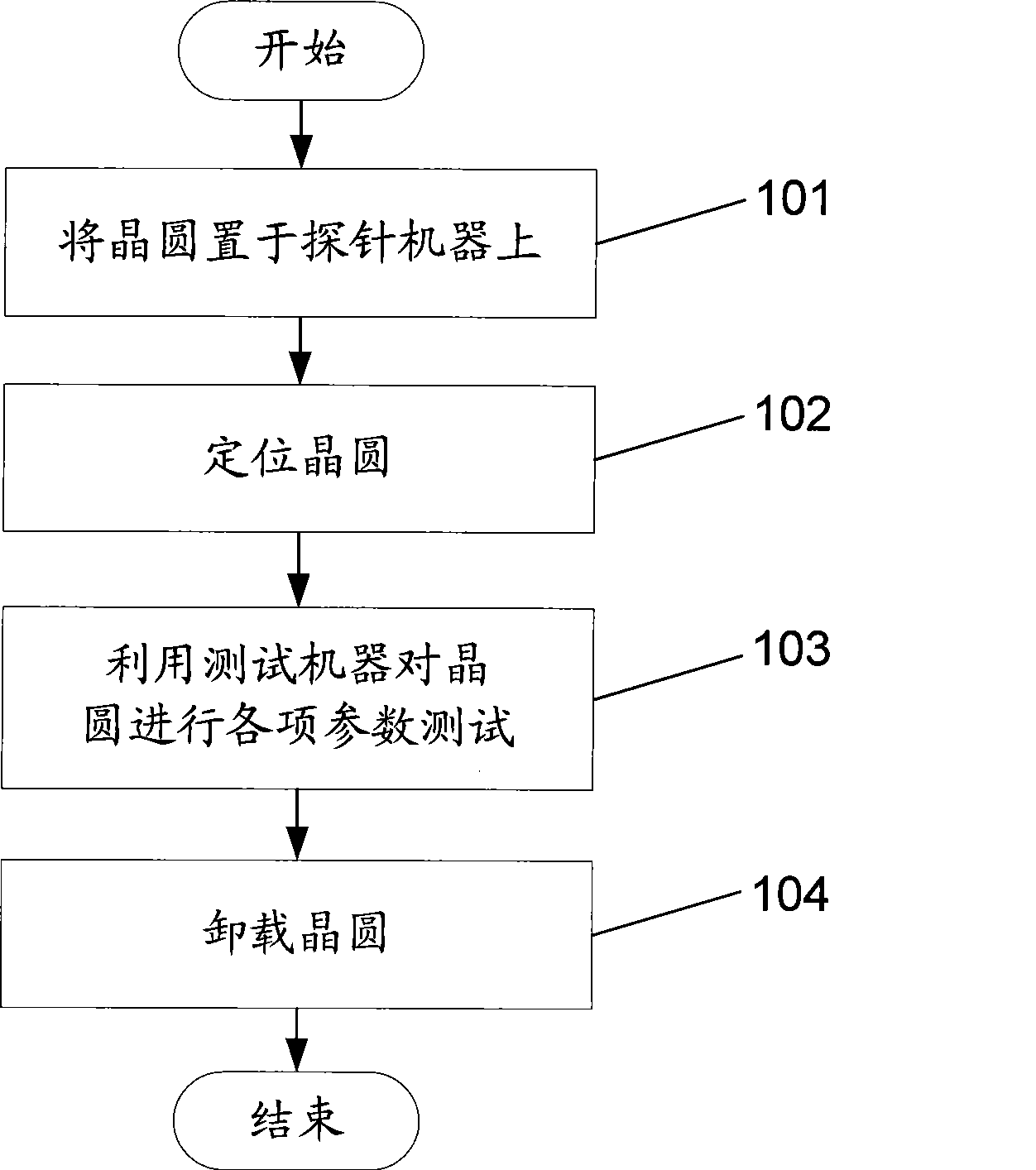
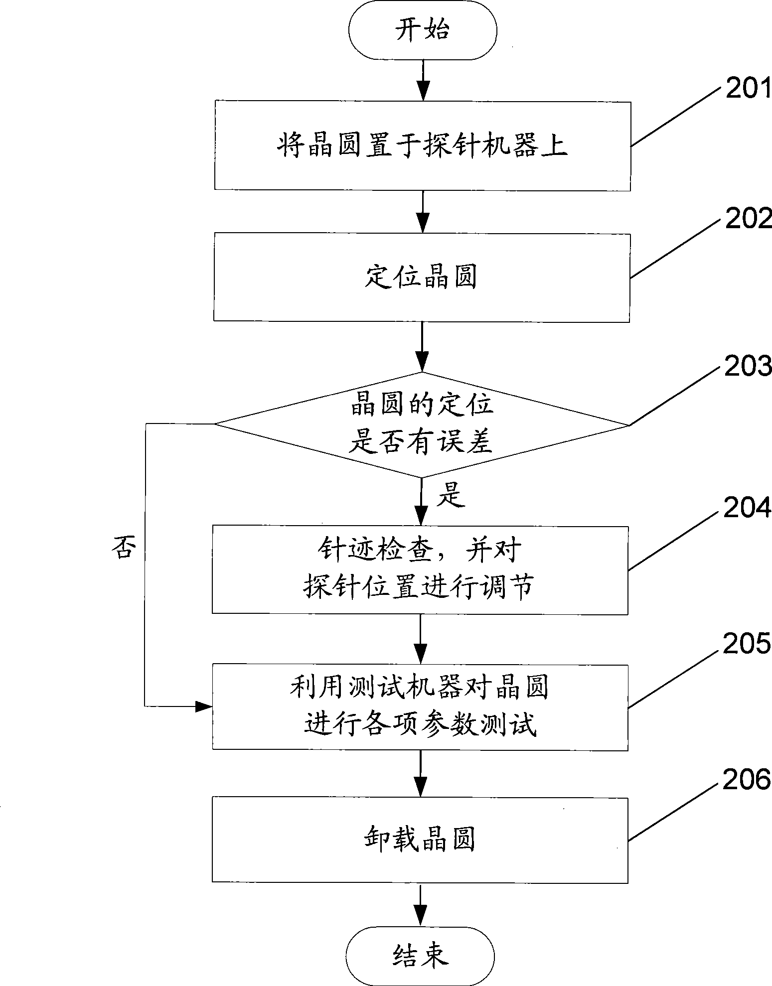
[0036] figure 2 It is the WAT flowchart of the present invention. The test steps for each wafer are as follows:

[0037] 201) placing the wafer on the probe machine (Prober);

[0038] 202) Alignment wafer;

[0039] 203) Determine whether there is an error in the positioning of the wafer, if there is an error, perform step 204); if there is no error, perform step 205);

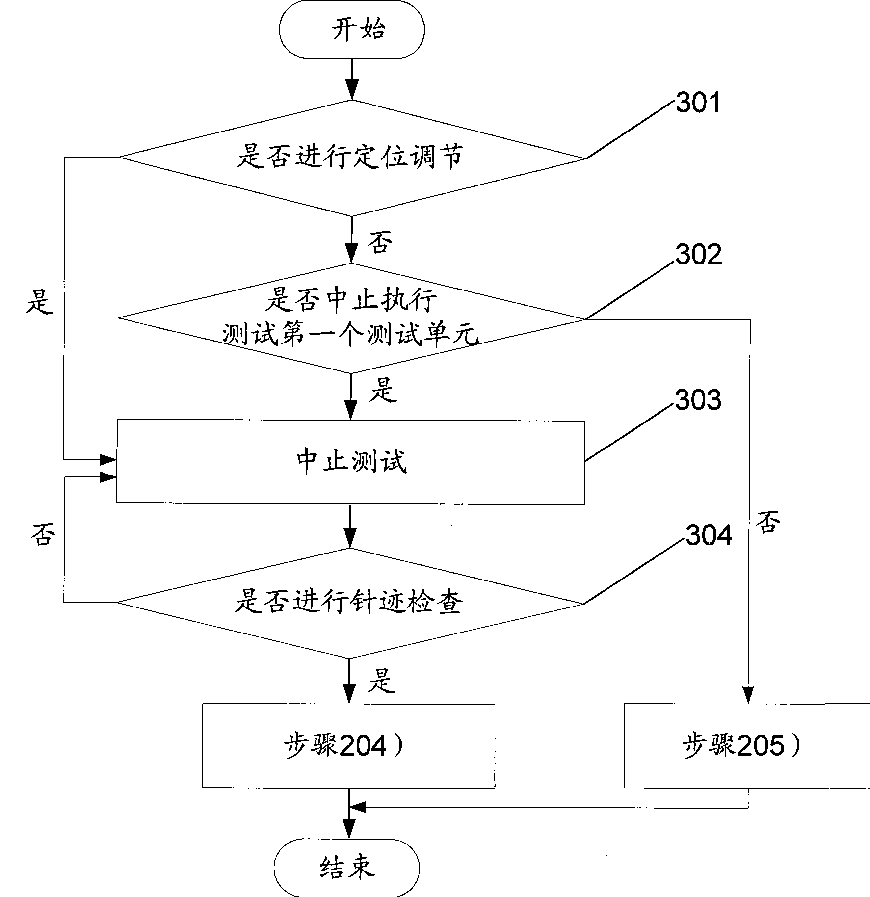
[0040] 204) Stitch checking, and adjusting the position of the probe;

[0041] 205) using a tester (Tester) to perform various parameter tests on the wafer;

[0042] 206) Unloading the wafer.

[0043] The method of the present invention monitors the wafer positioning through the microscope (Camera) of the probe machine, and if the wafer positioning is correct, then perform step 205), that is, the testing steps for each wafer are consistent with the steps of the prior art, If...


PUM


Abstract

The invention discloses a method for eliminating probe track offset, which is characterized in that the method comprises following steps: A) a wafer can be arranged on a probe device; B) the wafer is positioned; C) whether the wafer position has errors or not is judged, if yes, and then step D can be executed; if no error exists, step E is executed; D) the probe trace is detected, and the probe position can be adjusted; E) all parameters of the wafer can be tested through a test machine; F) the wafer is unloaded. The method belongs to the integration circuit manufacturing, can greatly reduce error of the measuring result of electrical parameter, and can prevent the wafer from being discarded.

Description

technical field [0001] The invention relates to integrated circuit manufacturing technology, in particular to a method for eliminating probe mark shift in wafer acceptance test (WAT, Wafer Acceptance Test). Background technique [0002] Wafer Acceptance Test (WAT, Wafer Acceptance Test) is to understand and reflect the physical characteristics and manufacturing process of the entire wafer by measuring the electrical parameters of certain test component structures, so that early-stage R&D personnel can pass the above electrical parameters. The measurement results can improve the design and process of components. The electrical parameters include turn-on voltage, saturation current, leakage current, breakdown voltage of gate oxide layer, contact resistance, sheet resistance and the like. [0003] The results of semiconductor parameter testing need to be obtained through precise and fast parameter testing equipment, such as Tokyo Electron (TEL) probe machine (Prober), probe ca...

Claims


Application Information

Patent Timeline
Patent Type & Authority Applications(China)
IPC IPC(8): G01R31/00G01R31/26H01L21/66
Inventor 陈泰江吴鹏
Owner SEMICON MFG INT (SHANGHAI) CORP
Why Eureka
Try Eureka