Charge trapping memory cell with high speed erase

A charge capture and storage unit technology, applied in electrical components, circuits, electrical solid devices, etc., can solve problems such as limiting device operating variables, and achieve the effect of excellent data retention capabilities

Inactive Publication Date: 2009-02-18
MACRONIX INT CO LTD
View PDF5 Cites 5 Cited by
  • Summary
  • Abstract
  • Description
  • Claims
  • Application Information

AI Technical Summary

Problems solved by technology

However, the problem of erase saturation continues to limit the operating variables of the device
Also,

Method used


Image

  • Charge trapping memory cell with high speed erase
  • Charge trapping memory cell with high speed erase
  • Charge trapping memory cell with high speed erase

Examples


Embodiment Construction

[0075] Propose below according to preferred embodiment of the present invention, and supplement with Fig. 1 to Figure 15 as a detailed description of the invention.

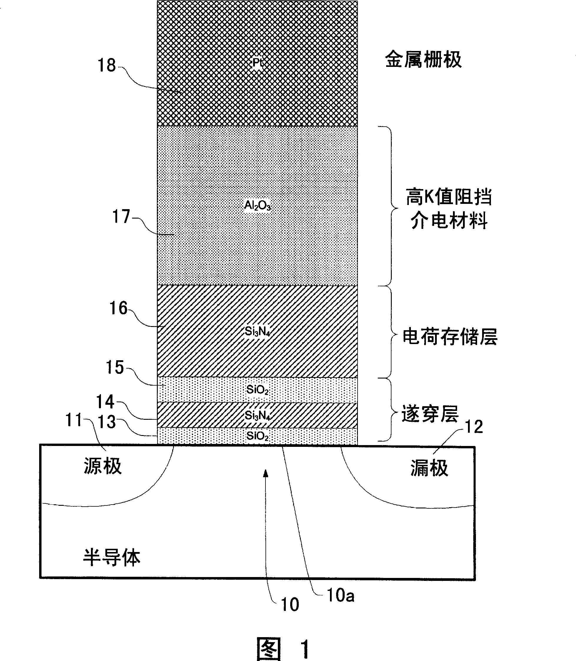
[0076] FIG. 1 is a schematic diagram of a charge trapping memory cell using a high-k blocking dielectric layer and a bandgap-engineered tunneling dielectric layer. The memory cell includes a channel 10 , a source 11 and a drain 12 in a semiconductor substrate. The source 11 and the drain 12 are adjacent to the channel 10 .

[0077] In this embodiment, the gate 18 includes platinum with a work function of about 8 electron volts (eV). In a preferred embodiment, the gate 18 is made of metal or metal compound, such as platinum, tantalum nitride, aluminum or other metal or metal compound gate material, preferably a material with a work function higher than 4.5 eV. A variety of high work function materials that may be suitable for use here as gate terminals are described in the above-mentioned US Patent No. 6,912,1...


PUM


Abstract

The invention discloses a charge trapping memory cell with high speed erase including a charge trapping element that is separated from a metal or metal compound gate through a blocking layer and separated from a semiconductor substrate comprising a channel through a processing tunneling dielectric material. The blocking layer is a material having a high dielectric constant, such as aluminum oxide. The metal or metal compound gate is such as platinum metal gate. Fast program and erase speeds with memory window as great as 7 V are achieved by the charge trapping memory cell.

Description

technical field [0001] The present invention relates to flash memory technology, and more particularly to a scalable charge trapping memory technology suitable for high speed erase and program operations. Background technique [0002] Flash memory (flash memory) is a type of non-volatile integrated circuit memory technology. Traditional flash memory uses floating gate memory cells. As the integration level of memory devices increases, the floating gate memory cells become closer together, making mutual interference of charges stored in adjacent floating gates gradually becoming a problem. Therefore, the ability to increase the integration level of the flash memory based on the floating gate memory cell is limited. Another type of memory cell used in flash memory is a charge trapping memory cell that utilizes a dielectric charge trapping layer instead of a floating gate. The charge-trapping memory cell uses a dielectric charge-trapping material, which does not cause interfe...

Claims


Application Information

Patent Timeline
IPC IPC(8): H01L27/115H01L29/792H01L29/49H01L29/51
CPCH01L29/4234H01L29/66833H01L29/792H10B63/80H10B43/30
Inventor 吕函庭赖升志
Owner MACRONIX INT CO LTD
Why Eureka
Try Eureka