Double-layer doping-layer silicon-based film solar cell

A silicon-based thin film, solar cell technology, applied in circuits, photovoltaic power generation, electrical components, etc., can solve the problems of increasing the steps and complexity of the battery manufacturing process, the influence of the overall performance of the battery, and the inability to suppress the particle exchange. Improve fill factor and initial photoelectric conversion efficiency, improve open circuit voltage and light stability, and improve the effect of light stability

Inactive Publication Date: 2009-02-25
SOUTH WEST INST OF TECHN PHYSICS
View PDF0 Cites 12 Cited by
  • Summary
  • Abstract
  • Description
  • Claims
  • Application Information

AI Technical Summary

Problems solved by technology

At present, in response to the above situation, many process technologies have emerged, such as buffer layers, barrier layers, etc., but these process technologies can only solve part of the above problems. For example, simple buffer layer growth technology can improve the problem of increased defects at the interface, but The exchange effect of particles between the doped layer and the intrinsic layer cannot be suppressed, and the common barrier layer technology will introduce new impurities
Although microcrystalline silicon, including nanocrystalline thin film cells, has been significantly improved in terms of interface defects, the overall performance of the cell is still severely affected by the exchange of particles between the doped layer and the intrinsic layer.
The simple combination of buffer layer, barrier layer and nanocrystalline or microcrystalline silicon film growth technology increases the steps and complexity of the battery manufacturing process, resulting in a significant increase in battery manufacturing costs

Method used


Image

  • Double-layer doping-layer silicon-based film solar cell
  • Double-layer doping-layer silicon-based film solar cell
  • Double-layer doping-layer silicon-based film solar cell

Examples


Embodiment Construction

[0022] Below in conjunction with accompanying drawing and embodiment the specific embodiment of the present invention is described in further detail:

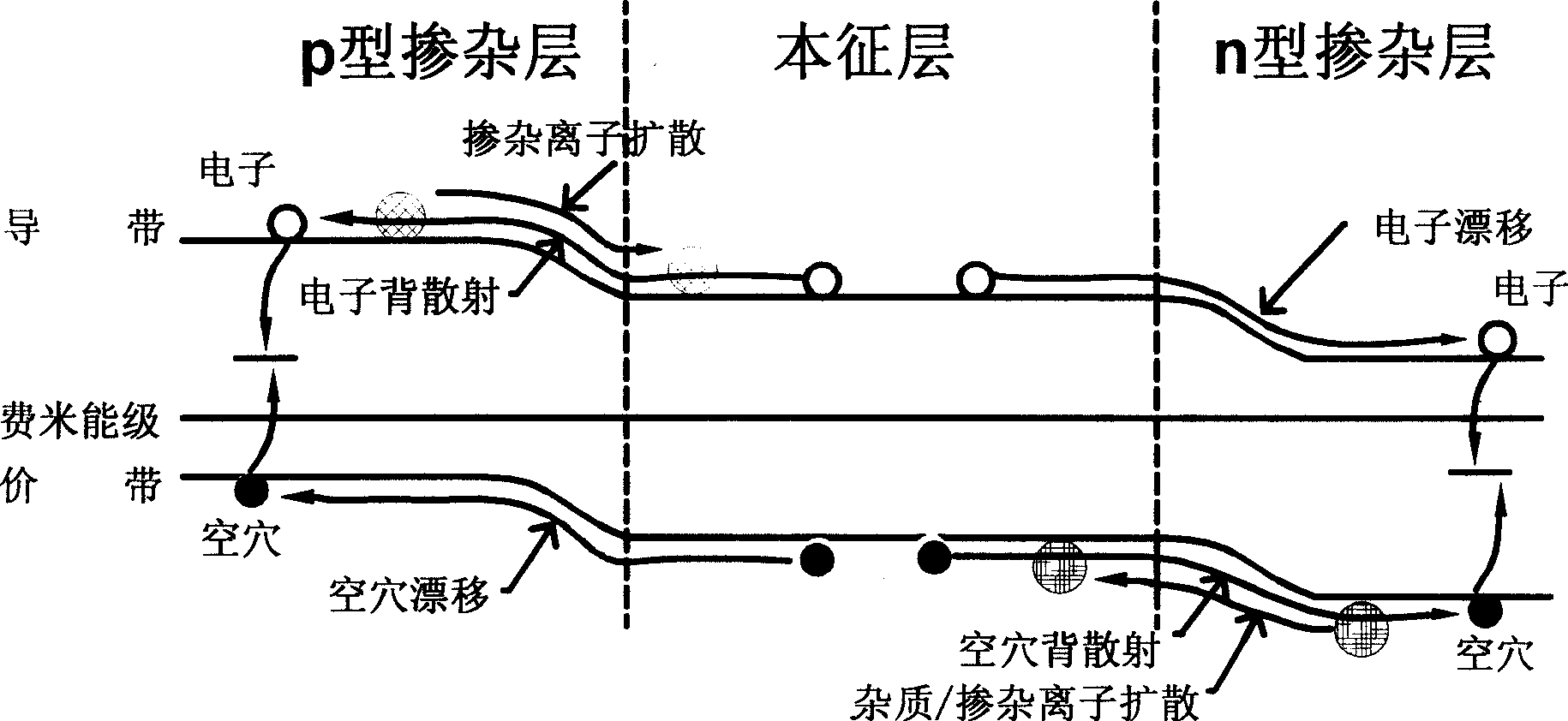
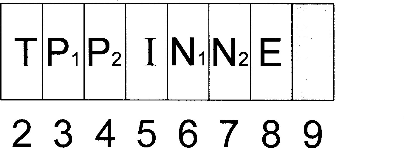
[0023] refer to figure 2 , image 3 . In the single-junction doped layer silicon-based thin film solar cell embodiment, figure 2 The p-i-n structure silicon-based thin film solar cell shown is fabricated on a transparent substrate, image 3 The shown n-i-p type silicon-based thin film solar cell is fabricated on an opaque substrate.

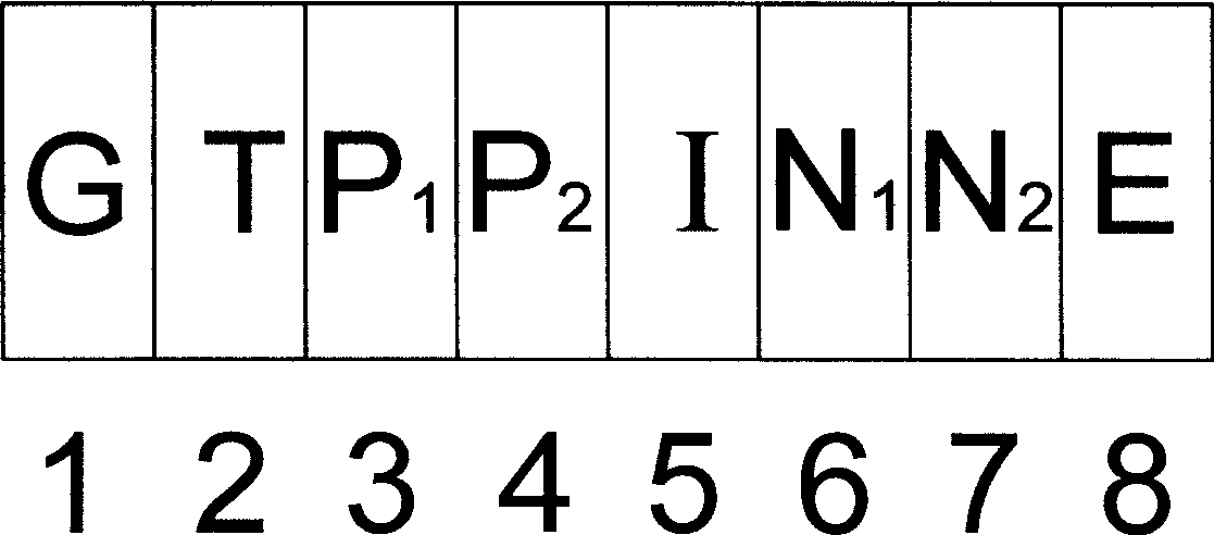
[0024] When the p-i-n type structure is adopted, the SnO with textured structure using transparent conductive glass as the transparent substrate 1 2 :F on the transparent conductive film 2, first deposit a boron-doped p-type silicon-doped layer 3 with a thickness of 15.0-25.0nm, the specific material is p-type boron-doped microcrystalline silicon, and the deposition of this layer adopts PECVD technology, basically The deposition condition is 13.56~100MHz high-frequency glow excitation, grea...


PUM


Abstract

The invention relates to a double doped layer silicon-based film solar cell. In a p type doped layer and an n type doped layer, the optical band gap of the layer closely adjacent to an intrinsic layer is larger than that of the layer far away from the intrinsic layer, but the difference value of the band gaps is not larger than 0.45 eV. The difference of the optical band gaps of the double doped layer structure is realized by arranging different materials according to the matching principle, or by changing the growth technology parameter of the identical material to control the optical band gaps. According to the invention, the inhibition to the particle interaction at the interface between the doped layers and the intrinsic layer and the control to the dopant particles and the accumulation and the distribution of defects can be realized simultaneously, excessive defects in the intrinsic layer can be reduced, simultaneously, the initial photoelectric conversion efficiency and the irradiation stability of the solar cell can be improved, the production cost for the silicon-based film solar cells can be further reduced, therefore, the structure can be applied to any silicon-based single-junction solar cell, laminated solar cell and multi-junction solar cell with p-i-n structure and n-i-p structure.

Description

technical field [0001] The invention relates to a thin-film solar cell with a silicon-doped layer structure, in particular to a p-type and n-type doped layer silicon-based thin-film solar cell with a double-layer structure composed of layers with different optical band gaps. Background technique [0002] The current silicon-based thin-film solar cells mainly refer to amorphous silicon cells, and the technological progress in the initial stage involves ① using a gradient interface layer to improve the transport characteristics of the junction interface. ②Use suede SnO 2 : F or ZnO replaces the planar ITO transparent conductive film, and adopts a multi-layer back reflection electrode to reduce light reflection and transmission loss and improve short-circuit current. ③The stacked battery structure is adopted to expand the spectral response range of the battery and improve the conversion efficiency. All these new technologies have increased the efficiency of silicon-based thin...

Claims


Application Information

Patent Timeline
Patent Type & Authority Applications(China)
IPC IPC(8): H01L31/075H01L31/0248H01L31/076
CPCY02E10/50Y02E10/548
Inventor 余晨辉余丽波覃文治石柱王鸥
Owner SOUTH WEST INST OF TECHN PHYSICS
Why Eureka
Try Eureka