Non-volatile memory of multi-layered nano-crystal floating gate structure

A non-volatile, nanocrystalline technology, used in semiconductor/solid-state device manufacturing, transistors, semiconductor devices, etc., can solve problems such as storage window not reaching industrial mass production, device threshold voltage changes, etc., to achieve short programming time, read and write The effect of low voltage and large storage window

Inactive Publication Date: 2009-03-11
INST OF MICROELECTRONICS CHINESE ACAD OF SCI
View PDF0 Cites 10 Cited by
  • Summary
  • Abstract
  • Description
  • Claims
  • Application Information

AI Technical Summary

Problems solved by technology

[0006] In such nanocrystalline floating-gate memories, charges are directly tunneled into the nanocrystal grains resulting in a change in the device threshold voltage
However, the current charge storage time and storage window of nanocrystalline memory have not yet met the needs of industrial mass production, and there is an urgent need for the emergence of nanocrystalline floating gate memory based on new structures

Method used


Image

  • Non-volatile memory of multi-layered nano-crystal floating gate structure
  • Non-volatile memory of multi-layered nano-crystal floating gate structure
  • Non-volatile memory of multi-layered nano-crystal floating gate structure

Examples


Embodiment Construction

[0039] In order to make the object, technical solution and advantages of the present invention clearer, the present invention will be described in further detail below in conjunction with specific embodiments and with reference to the accompanying drawings.

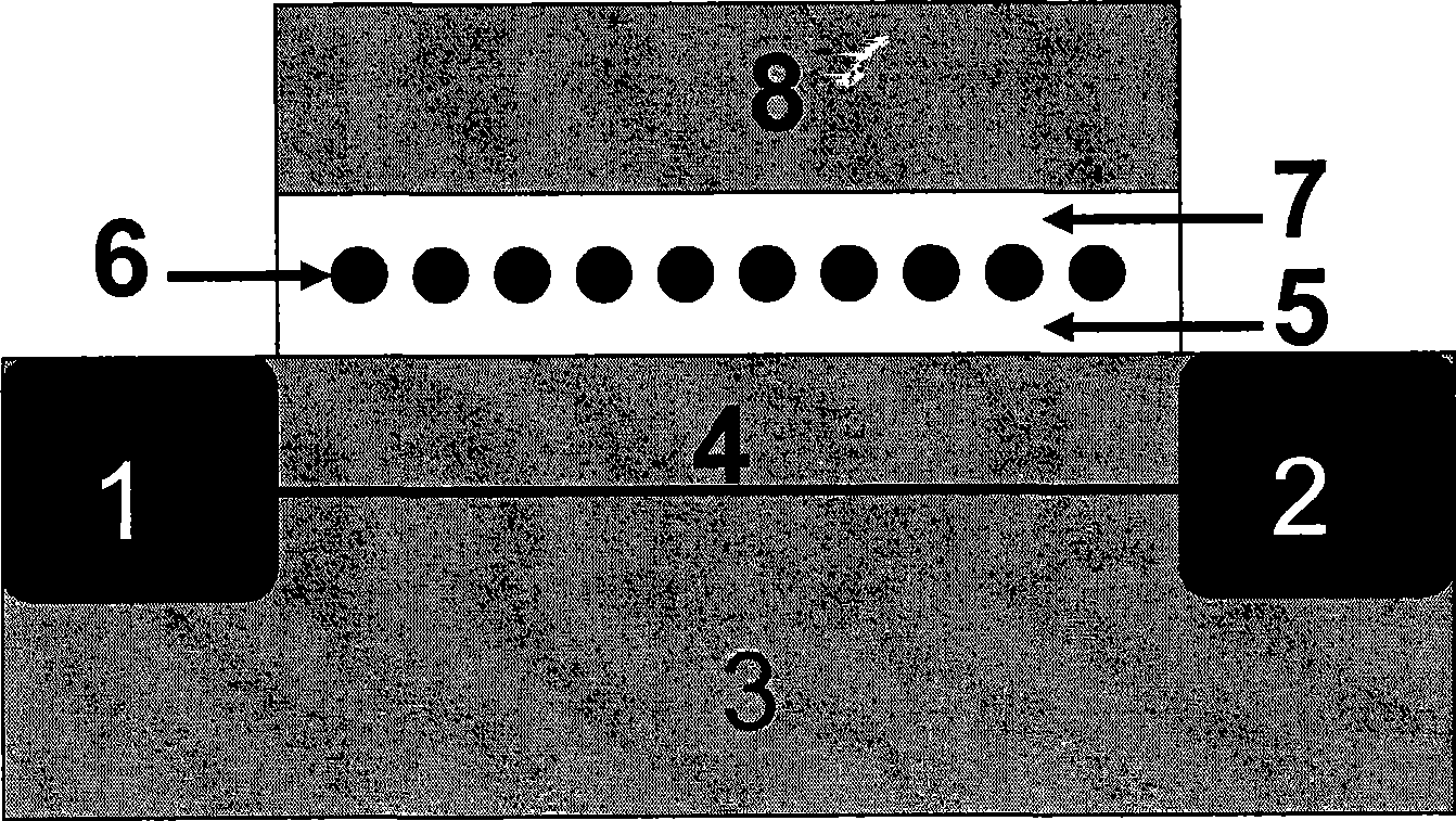
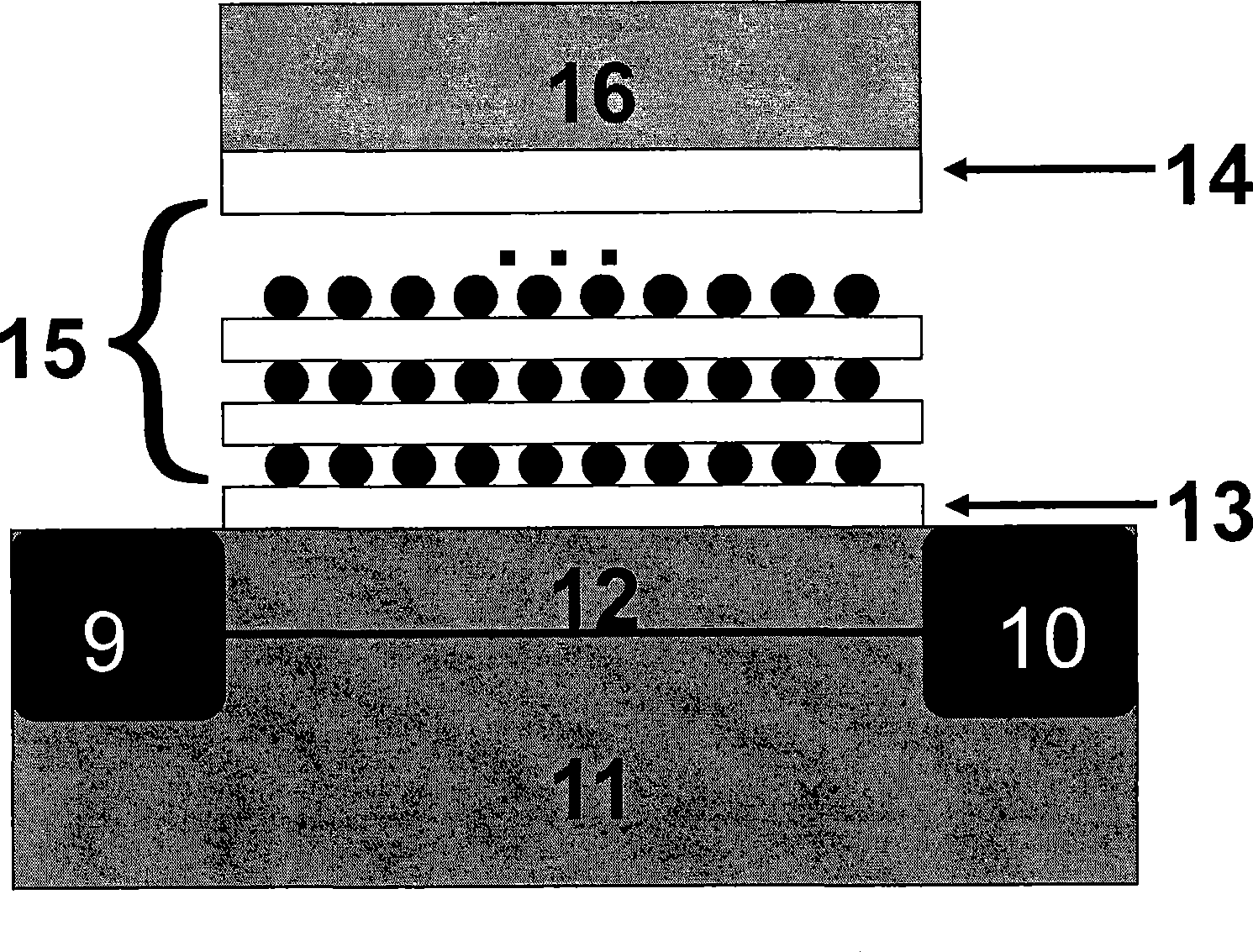
[0040] Such as figure 2 as shown, figure 2 Schematic diagram of the structure of the multi-layer nanocrystalline floating gate structure non-volatile memory provided by the present invention, the non-volatile memory includes: a semiconductor substrate 11 for supporting the entire non-volatile memory; doping in the semiconductor substrate 11 to form A source 9 and a drain 10; a channel 12 between the source 9 and the drain 10; a tunnel oxide layer 13 on the channel 12; a control oxide layer for controlling the oxidation of the multilayer nanocrystalline floating gate structure 14 ; the multilayer nanocrystalline floating gate structure 15 located between the tunnel oxide layer 13 and the control oxide layer 14 ; the gat...


PUM


Abstract

The invention discloses a nonvolatile memory with a multi-layer nanocrystal floating gate structure, which belongs to the technical field of the nonvolatile memory. The nonvolatile memory comprises a semiconductor substrate 11 used for supporting the entire nonvolatile memory, a source 9 and a drain 10 which are formed in the semiconductor substrate 11 in a doped way, a channel 12 between the source 9 and the drain 10, a tunneling oxidizing layer 13 positioned on the channel 12, a control oxidizing layer 14 used for controlling oxidation of the multi-layer nanocrystal floating gate structure, a gate electrode 16 positioned on the control oxidizing layer 14 and a multi-layer nanocrystal floating gate structure 15 positioned between the tunneling oxidizing layer 13 and the control oxidizing layer 14 and used as the floating gate storage unit of the nonvolatile memory. The invention also discloses a method for preparing the nonvolatile memory with the multi-layer nanocrystal floating gate structure. The invention solve the contradiction between the programming time/voltage of the single-layer nanocrystal floating gate memory and the storage time, and increases the storage time of the element under the precondition of shorter programming time.

Description

technical field [0001] The invention relates to the technical field of non-volatile memory in integrated circuits, in particular to a non-volatile memory with a multilayer nanocrystal floating gate structure and a preparation method thereof. Background technique [0002] In recent years, the growth rate of memory in integrated circuits has exceeded that of logic circuits. The proportion of memory in chip area has increased from 20% in 1999 to 71% in 2005, while logic circuits have decreased from 66% in 1999 to 2005. 16%. [0003] Among memory products, the fastest growing market demand is non-volatile memory. As a typical device of non-volatile memory, flash memory (FlashMemory) has been widely used in various handheld mobile storage electronic products such as U disk, MP3 player and mobile phone. However, the flash memory device structure widely adopted by the industry is facing serious challenges in terms of storage time and power consumption while developing to nanomete...

Claims


Application Information

Patent Timeline
Patent Type & Authority Applications(China)
IPC IPC(8): H01L29/788H01L29/49H01L27/115H01L21/336H01L21/28H01L21/8247
Inventor 王琴管伟华刘琦胡媛李维龙龙世兵贾锐陈宝钦刘明
Owner INST OF MICROELECTRONICS CHINESE ACAD OF SCI
Why Eureka
Try Eureka