Accumulation layer controlled insulation gate type bipolar transistor

A technology of bipolar transistors and accumulation layers, applied in semiconductor devices, electrical components, circuits, etc., can solve the problems of increased amplification factor of PNP transistors, increased resistance of P-type base area 8, and reduced safe operating area, etc., to achieve Improved reliability and high-temperature operating characteristics, good turn-off loss, and reduced manufacturing costs

Inactive Publication Date: 2009-03-25
UNIV OF ELECTRONICS SCI & TECH OF CHINA
View PDF0 Cites 18 Cited by
  • Summary
  • Abstract
  • Description
  • Claims
  • Application Information

AI Technical Summary

Problems solved by technology

However, when the trench gate type insulated gate bipolar transistor works at high temperature, on the one hand, due to the increase in temperature, the carrier lifetime increases, and the amplification factor of the PNP transistor becomes larger, resulting in a larger hole current flowing through the P-type base region 8 ; On the other hand, the increase in temperature makes the mobility of holes greatly reduced, and the resistance of the P-type base region 8 increases; both reasons will cause the traditional trench insulated gate bipolar transistor to resist latch-up due to the increase in temperature. The ability is greatly reduced, the safe working area is also reduced, and the reliability is reduced. How to find better high temperature anti-latch-up ability is an urgent problem to be solved

Method used


Image

  • Accumulation layer controlled insulation gate type bipolar transistor
  • Accumulation layer controlled insulation gate type bipolar transistor
  • Accumulation layer controlled insulation gate type bipolar transistor

Examples


Embodiment Construction

[0041] By adopting the accumulation layer control structure of the present invention, an insulated gate bipolar transistor with low conduction voltage drop, high current density, large safe operating area, low cost, and a better compromise between conduction voltage drop and turn-off loss can be obtained . It can be applied to planar gate structure, trench gate structure and lateral structure, etc. With the development of semiconductor technology, more power devices with low voltage drop, high current and high reliability can be produced by adopting the invention.

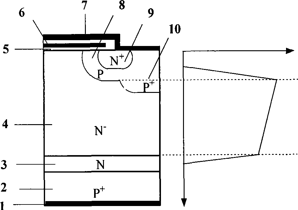
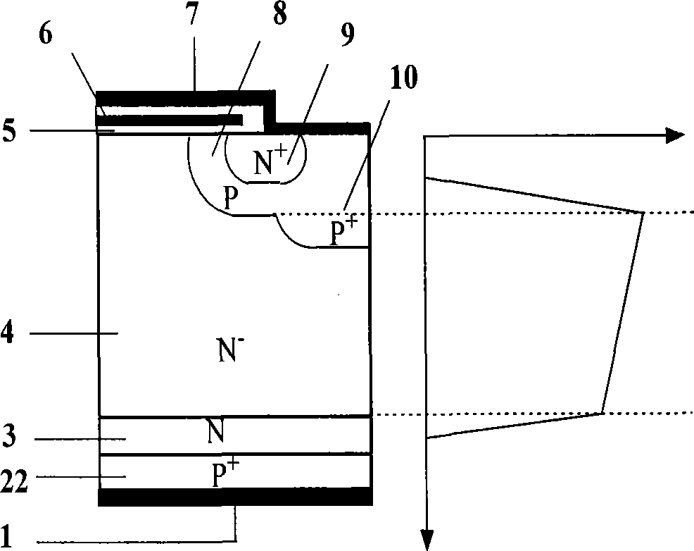
[0042] Trench insulated gate bipolar transistors that introduce accumulation layer control structures, such as Figure 5 shown, including collector 1, P-type collector 23, N - Base region 4, gate oxide layer 5, polysilicon gate 6, emitter 7, N + Source region 9, P + body area 10.

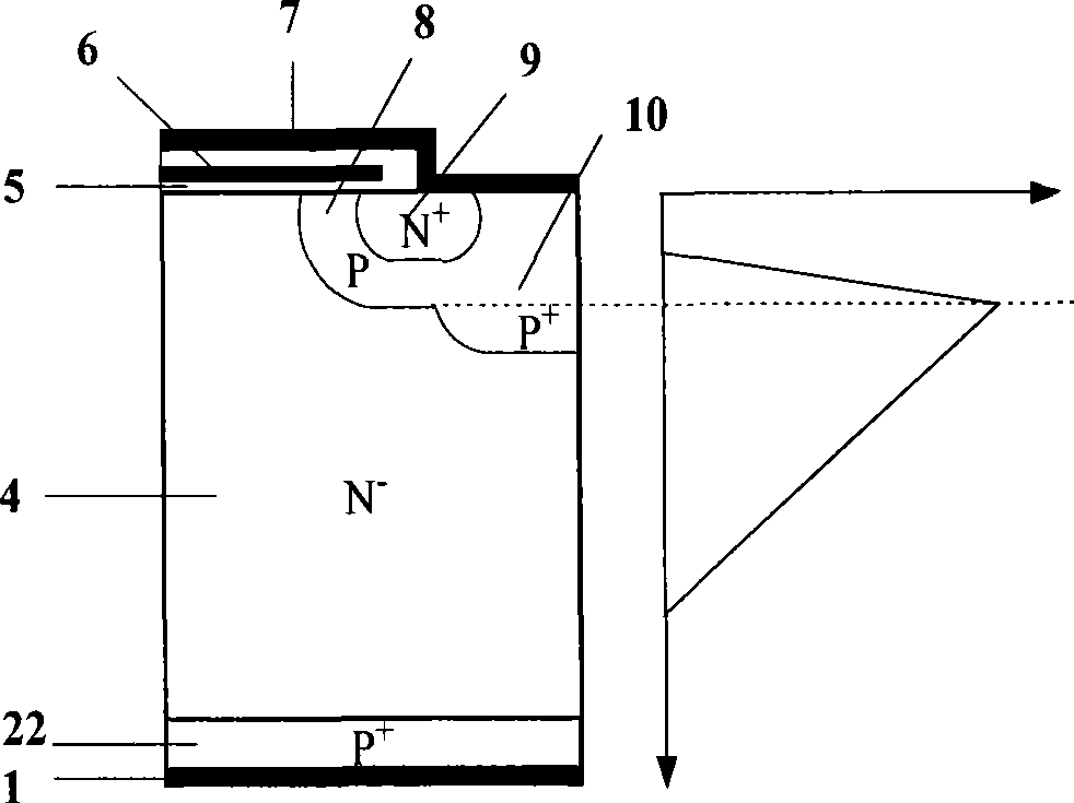
[0043] An accumulation layer controlled planar gate insulated gate bipolar transistor, such as Image 6 shown, including collecto...


PUM


Abstract

Insulated gate bipolar transistors controlled by an accumulation layer belong to the technical field of semiconductor power devices. The transistors include a channel insulated gate bipolar transistor, a plane insulated gate bipolar transistor and a transverse insulated gate bipolar transistor. According to the invention, when a device is in the blocking state, a built-in electric field formed by a P body region (10) and an N base region (4) forms part of an electron barrier which stops electrons flowing from an N source region (9) into the N base region(4) with the voltage-resistance of the device improved; when the device is in the conductive state, the accumulation layer is formed between the N source region (4) and a gate oxide layer (5), and the electrons can flow from the N source region (9) to the N base region (4) through the accumulation layer so as to control the normal operation of the device. With the accumulation layer rather than a P-type base region and an MOS inversion channel of a traditional insulated gate bipolar transistor, the invention can achieve lower conductive voltage drop and greater saturation current density, thereby avoiding parasitic thyristor effect, and ensuring that the safe operating area, the reliability and the high-temperature working characteristics of the device can be greatly promoted.

Description

technical field [0001] An insulated gate bipolar transistor controlled by an accumulation layer belongs to the technical field of semiconductor power devices. Background technique [0002] Insulated gate bipolar transistor is a rapidly developing and widely used power electronic device. It is a new device combined with the advantages of high input impedance of MOSFET, simple driving circuit, high current density and low saturation voltage of bipolar transistor. Now it is widely used in induction cooker, UPS uninterruptible power supply, automotive electronic igniter, frequency converter, motor transmission system and other energy conversion devices. [0003] IGBT was first proposed in 1982 as a punch-through structure, such as figure 1 As shown, it is at high concentrations of P + On the substrate 2, the N-type buffer layer 3, N - The base region layer 4 is fabricated into an insulated gate bipolar transistor structure. Due to the presence of the N-type buffer layer 3, ...

Claims


Application Information

Patent Timeline
Patent Type & Authority Applications(China)
IPC IPC(8): H01L29/739H01L29/06
Inventor 李泽宏钱梦亮张波
Owner UNIV OF ELECTRONICS SCI & TECH OF CHINA
Why Eureka
Try Eureka