Monolithic integrated phase inverter based on GaN-based enhanced device and preparation method thereof

A monolithic integrated, enhancement-mode technology, applied in semiconductor/solid-state device manufacturing, semiconductor devices, electrical components, etc., can solve the problem of high on-resistance of p-channel enhancement-mode heterostructure field effect transistors, hindering GaN-based inversion It can improve the hole mobility, increase the threshold voltage, and reduce the on-resistance due to problems such as the application of devices and monolithic integrated circuits, and the large leakage of the gate electrode.

Pending Publication Date: 2022-04-29
西安电子科技大学广州研究院
View PDF0 Cites 0 Cited by
  • Summary
  • Abstract
  • Description
  • Claims
  • Application Information

AI Technical Summary

Problems solved by technology

[0005] However, there are still a lot of problems in this inverter: the on-resistance of the p-channel enhancement heterostructure field effect transistor is relatively high, the threshold voltage is relatively low, and the gate electrode leakage of its monolithically integrated n-channel GaN enhancement device is relatively low. Large, low gate voltage swing, which hinders the application of GaN-based inverters and monolithic integrated circuits in power electronic systems

Method used


Image

  • Monolithic integrated phase inverter based on GaN-based enhanced device and preparation method thereof
  • Monolithic integrated phase inverter based on GaN-based enhanced device and preparation method thereof
  • Monolithic integrated phase inverter based on GaN-based enhanced device and preparation method thereof

Examples


Embodiment 1

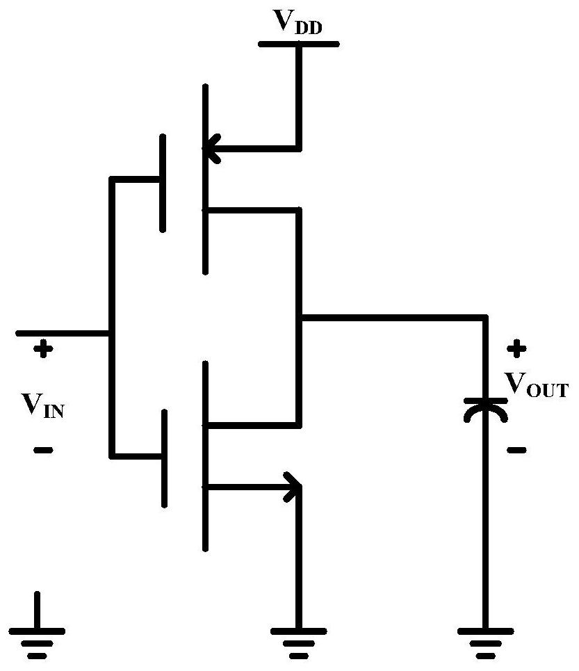
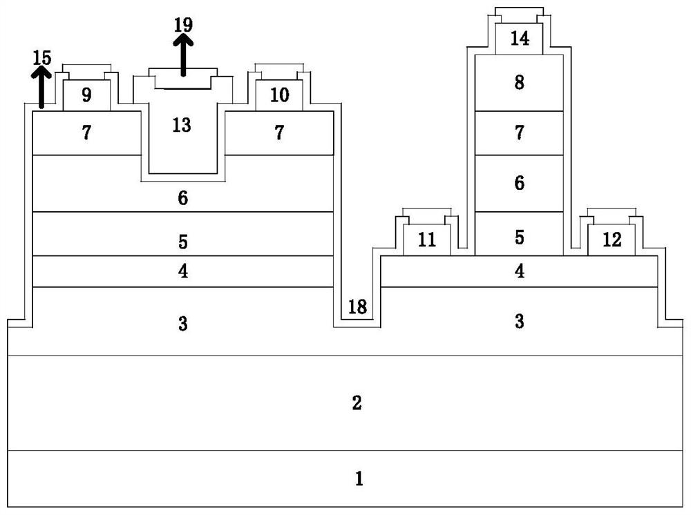
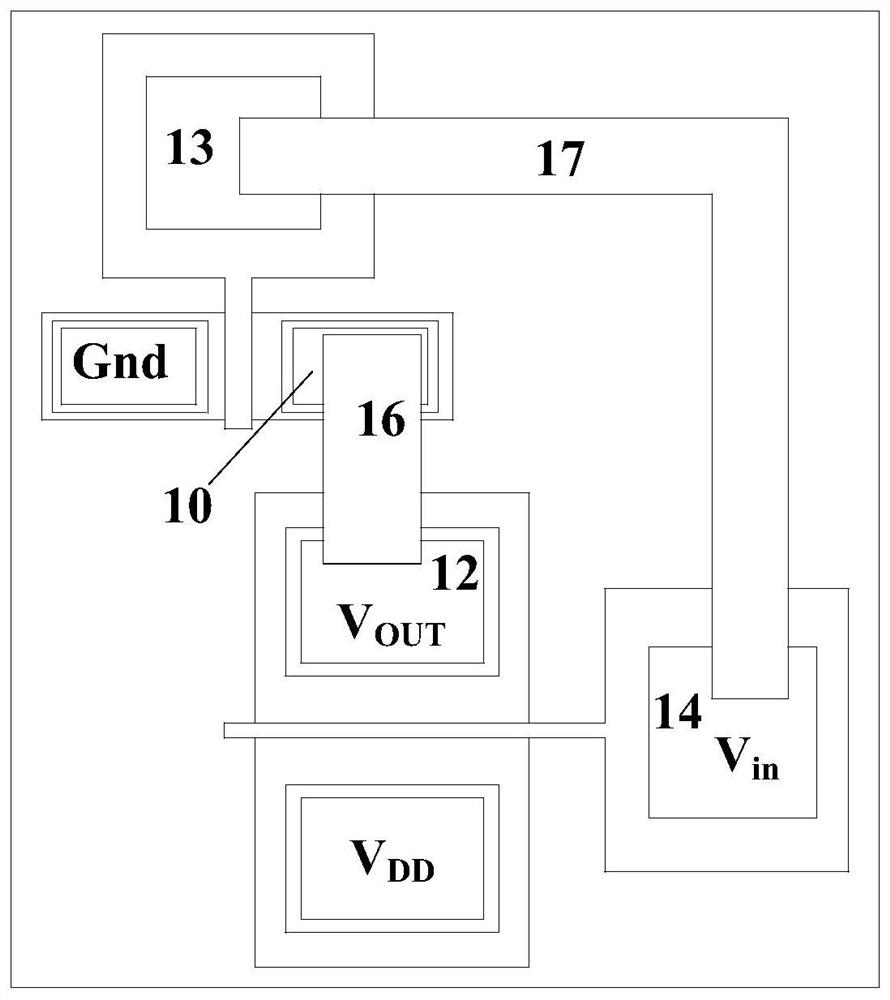
[0042] See figure 2 , figure 2 It is a schematic structural diagram of a monolithic integrated inverter based on a GaN-based enhancement device provided by an embodiment of the present invention, which sequentially includes a substrate 1, a buffer layer 2, a UID-GaN layer 3, and an AlGaN barrier layer from bottom to top 4. The UID-InGaN layer 5 and the p-InGaN layer 6. An isolation groove 18 as deep as the UID-GaN layer is provided in the middle of the device to divide the device into left and right parts; wherein,

[0043] The p-InGaN layer 6 on the left side of the device is provided with a first source electrode 9 and a first drain electrode 10, and a first gate as deep as the p-InGaN layer 6 is provided between the first source electrode 9 and the first drain electrode 10. An electrode 13 to form a p-channel enhancement type heterostructure field effect transistor;

[0044] A second source electrode 11 and a second drain electrode 12 are provided on the AlGaN barrier l...

Embodiment 2

[0058] On the basis of the first embodiment above, this embodiment provides a method for manufacturing a monolithic integrated inverter based on p-channel and n-channel GaN-based enhancement devices. See Figure 4 , Figure 4 It is a flow chart of a method for manufacturing a monolithic integrated inverter based on a GaN-based enhancement device provided by an embodiment of the present invention, specifically including:

[0059] Step 1: Epitaxial buffer layer, UID-GaN layer, AlGaN barrier layer, UID-InGaN layer and p-InGaN layer on the substrate in sequence.

[0060] Specifically, in this embodiment, a metal-organic chemical vapor deposition process is used to sequentially grow various layer structures on a silicon substrate to obtain a silicon substrate.

[0061] Step 2: Etching the right side of the substrate to form the gate region of the n-channel enhancement type heterostructure field effect transistor.

[0062] Specifically, photolithography and inductively coupled pl...

Embodiment 3

[0092] The process of the preparation method provided by the present invention will be described in detail below in conjunction with the accompanying drawings.

[0093] See Figures 5a-5m , Figures 5a-5m It is a process schematic diagram of a method for manufacturing a monolithic integrated inverter based on a GaN-based enhancement device provided by an embodiment of the present invention. This embodiment includes UID-InGaN layer, p-InGaN layer, p + -InGaN layer and n-GaN layer devices are taken as examples to introduce the preparation process, which specifically includes the following steps:

[0094] S1: Prepare n-GaN / p-InGaN / AlGaN / GaN / silicon substrate substrate.

[0095] Using metal organic chemical vapor deposition process, epitaxial GaN buffer layer, UID-GaN, AlGaN barrier layer, UID-InGaN, p-InGaN layer, p + -InGaN layer and n-GaN layer to obtain n-GaN / p-InGaN / AlGaN / GaN / silicon substrate substrate, such as Figure 5a shown.

[0096] S2: n-GaN etching

[0097] Usi...


PUM

PropertyMeasurementUnit
thicknessaaaaaaaaaa
thicknessaaaaaaaaaa
thicknessaaaaaaaaaa

Abstract

The invention discloses a monolithic integrated inverter based on a GaN-based enhanced device and a preparation method thereof, the inverter sequentially comprises a substrate, a buffer layer, a UID-GaN layer, an AlGaN barrier layer, a UID-InGaN layer and a p-InGaN layer from bottom to top, and an isolation groove deep to the UID-GaN layer is arranged in the middle of the device to divide the device into a left part and a right part; wherein a first source electrode and a first drain electrode are arranged on the p-InGaN layer on the left side of the device, and a first gate electrode which extends to the p-InGaN layer is arranged between the first source electrode and the first drain electrode, so that a p-channel enhanced heterostructure field effect transistor is formed; a second source electrode and a second drain electrode are arranged on the AlGaN barrier layer on the right side of the device, and a second gate electrode is arranged on the p-InGaN layer, so that the n-channel enhanced heterostructure field effect transistor is formed. According to the device provided by the invention, the saturation current density of the p-channel GaN enhanced device is improved, and the on-resistance is reduced; and meanwhile, the gate leakage of the n-channel GaN enhanced device is inhibited, and the gate voltage swing is improved.

Description

technical field [0001] The invention belongs to the technical field of semiconductor devices, and in particular relates to a monolithic integrated inverter based on a GaN-based enhanced device and a preparation method thereof. Background technique [0002] As a typical representative of the third-generation semiconductor, the bandgap semiconductor material gallium nitride (GaN) has the advantages of high electron mobility, high thermal conductivity, high breakdown electric field and strong radiation resistance, so that GaN-based heterojunction Structured power devices can obtain higher switching speed, higher blocking voltage, lower conduction loss and higher operating temperature, etc., and can work under harsh conditions such as high power, high frequency, high temperature and radiation . With the development of semiconductor technology, the research and development of GaN-based power transistors has made great progress. It has been widely used in the field of fast chargi...

Claims


Application Information

Patent Timeline
Patent Type & Authority Applications(China)
IPC IPC(8): H01L29/06H01L29/80H01L29/205H01L21/335
CPCH01L29/0607H01L29/66462H01L29/802H01L29/205
Inventor 张苇杭樊昱彤张进成刘茜付李煜黄韧许国富文钰郝跃张晓东
Owner 西安电子科技大学广州研究院
Why Eureka
Try Eureka