Method for improving ESD protection device uniform conduction

A device and uniform technology, which is applied in the field of improving the uniform conduction of ESD protection devices, can solve the problems such as the lack of obvious improvement in ESD protection tolerance and the realization of burdens due to high circuit integration, so as to improve ESD protection ability and large ESD Protection capability and the effect of reducing development costs

Inactive Publication Date: 2009-04-15
HEJIAN TECH SUZHOU
View PDF0 Cites 8 Cited by
  • Summary
  • Abstract
  • Description
  • Claims
  • Application Information

AI Technical Summary

Problems solved by technology

In general, after a few finger elements are turned on, the current can reach the current value of the secondary breakdown of the device, so in the entire ESD event, most of the finger elements are in the off state, so that even if the NMOSFET itself The size is very large, but its ESD protection tolerance has not been significantly improved, but it has become a burden to the realization of high integration of the circuit. Therefore, when Gated_NMOSFET is selected as the ESD protection device, how to increase the device size while making all indicators It is very critical that the like element can conduct uniformly

Method used


Image

  • Method for improving ESD protection device uniform conduction
  • Method for improving ESD protection device uniform conduction
  • Method for improving ESD protection device uniform conduction

Examples


no. 1 example

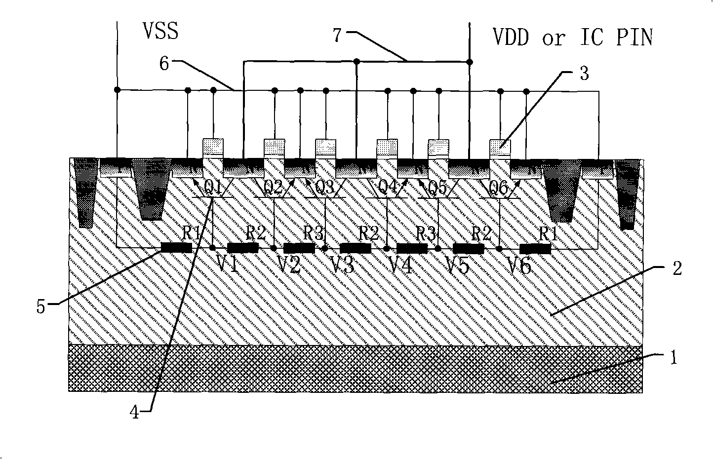
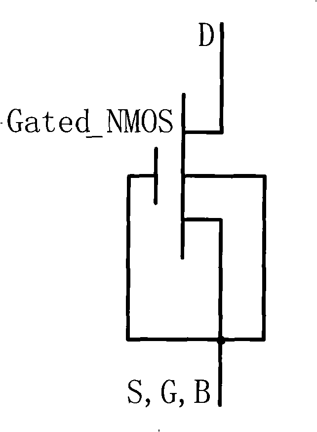
[0035] like image 3 The layout cross-sectional view of the ESD protection device under the implementation of high resistance for the method of the present invention to improve uniform conduction; as Figure 4 for image 3 Schematic diagram of the equivalent circuit of the device. image 3 In the same example, an NMOS transistor containing six finger elements is taken as an example, wherein the bottom end of the NMOS transistor is a P-type or N-type substrate 1, and there are multiple finger elements connected in parallel, which are respectively connected in parallel to the P well 2. The fingers are each associated with a parasitic triode 4 . As shown in the figure, it can be seen that the collectors of these parallel parasitic transistors (that is, the drain D of the NMOS transistor) are coupled to the working potential terminal VDD or the I / O terminal of the integrated circuit through the common drain line 7, and its The source S, the gate G and the substrate terminal B a...

no. 2 example

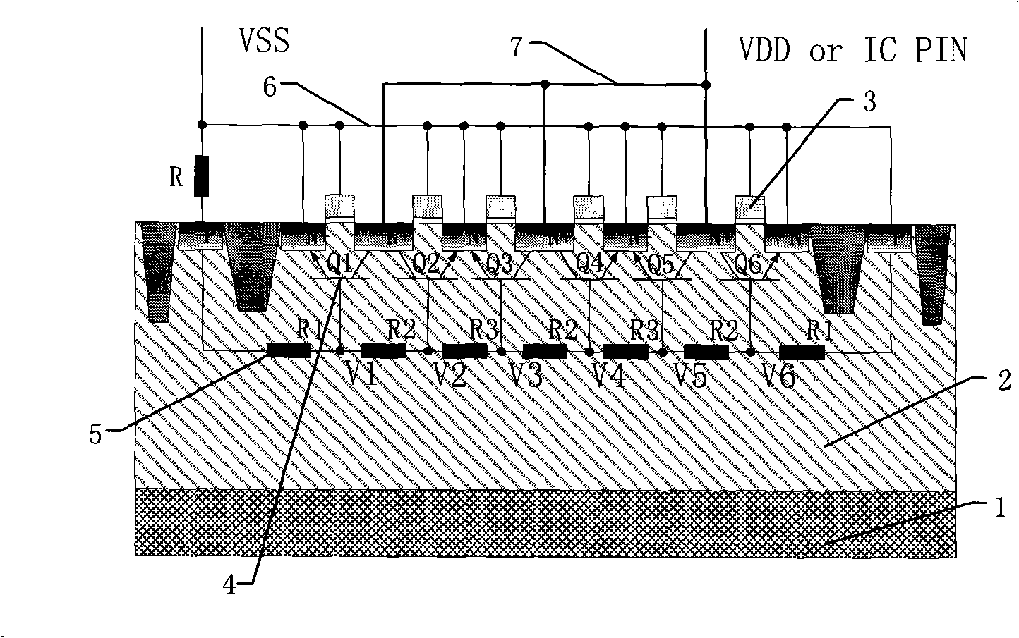
[0039] like Figure 5 The layout sectional view of the ESD protection device under the implementation of the diode for the method of the present invention to improve uniform conduction; as Figure 6 for Figure 5 Schematic diagram of the equivalent circuit of the device. The parts in the figure that are the same as those in the first embodiment will not be described here again, but different from the above-mentioned embodiments, the special feature of this embodiment is that a diode is used to replace the above-mentioned high resistance resistor R, and the anode of the diode is connected to the common ground The potential terminal VSS is coupled, and the cathode is coupled to the substrate terminal of the ESD protection device. When the drain of the NMOSFET transistor is forward-biased, the diode is in a reverse cut-off state. Due to its relatively high breakdown voltage, this high-resistance device can also make the base of the parasitic transistor in different positions T...


PUM


Abstract

The invention discloses a method for improving even conduction of an ESD protection device. The method is suitable for characteristic improvement of an electrostatic discharge (ESD) protection device in an integrated circuit, wherein, an MOS transistor is provided with a plurality of finger-shaped components which are connected with each other in parallel, and each of the finger-shaped component is respectively connected with a parasitic triode in parallel, and a collector electrode (i.e., a drain electrode of the MOS transistor) of each parasitic triode is coupled with an operating potential terminal or an I/O terminal of the integrated circuit by a common drain line; an emitter electrode (i.e., a source electrode of the MOS transistor) of the parasitic triode is connected with a common ground potential terminal together with a gate electrode and a substrate of the MOS transistor. The method is characterized in that: the substrate terminal of the MOS transistor is also serially connected with a high-resistance apparatus in the ESD protection device, and the substrate terminal of the MOS transistor is further coupled to the common ground potential terminal together with the source electrode and the gate electrode, which can reduce trigger voltage of Gated_MOSFET, causes a large-sized protection device to be more evenly conducted, improves the ESD protection capability of the device, and further reduces the circuit design area and lower the development cost.

Description

technical field [0001] The invention relates to an electrostatic discharge protection circuit, in particular to a method for improving the uniform conduction of an ESD protection device. Background technique [0002] With the increasingly advanced semiconductor manufacturing process, more and more designers pay more and more attention to the problem of electrostatic discharge (ElectroStatic Discharge). In circuit design, ESD protection devices that can be used are: resistors, diodes, triodes, metal oxide half field effect transistors and silicon controlled rectifiers, etc. Among a wide variety of ESD protection devices, Gated_MOSFET is the most widely used due to its ease of design and better protection capabilities. [0003] In particular, an N-type metal-oxide-semiconductor transistor (hereinafter referred to as NMOS) is an effective ESD protection device under the snapback breakdown mechanism. When ESD occurs, the snapback breakdown mechanism will cause the NMOS to cond...

Claims


Application Information

Patent Timeline
Patent Type & Authority Applications(China)
IPC IPC(8): H02H9/00H01L23/60
CPCH01L2924/0002
Inventor 石俊夏洪旭王政烈
Owner HEJIAN TECH SUZHOU
Why Eureka
Try Eureka