Electronic component and method for manufacturing the same

A technology of electronic components and manufacturing methods, which is applied in the direction of electrical components, electrical solid devices, semiconductor/solid device components, etc., can solve problems such as weak bonding force, bending and damage of bonding substrates, and achieve good productivity and realize productivity. Effect

Inactive Publication Date: 2009-04-15
MURATA MFG CO LTD
View PDF2 Cites 0 Cited by
  • Summary
  • Abstract
  • Description
  • Claims
  • Application Information

AI Technical Summary

Problems solved by technology

[0006] However, in the bonding structure disclosed in Patent Document 1, since two substrates are bonded by friction of the aluminum film caused by compression at room temperature, there is a problem of weak bonding force.
Therefore, when forming a chip by forming an element on a large substrate, bonding two substrates, cutting and chipping, there is a possibility that the bonded part may come off due to an impact during chip formation.
In addition, in the case where the element is sealed by such a junction, there is a possibility that cutting water may infiltrate into the element when the junction is cut off for chip formation.
In addition, in the case of the surface aco

Method used


Image

  • Electronic component and method for manufacturing the same
  • Electronic component and method for manufacturing the same
  • Electronic component and method for manufacturing the same

Examples


Example Embodiment

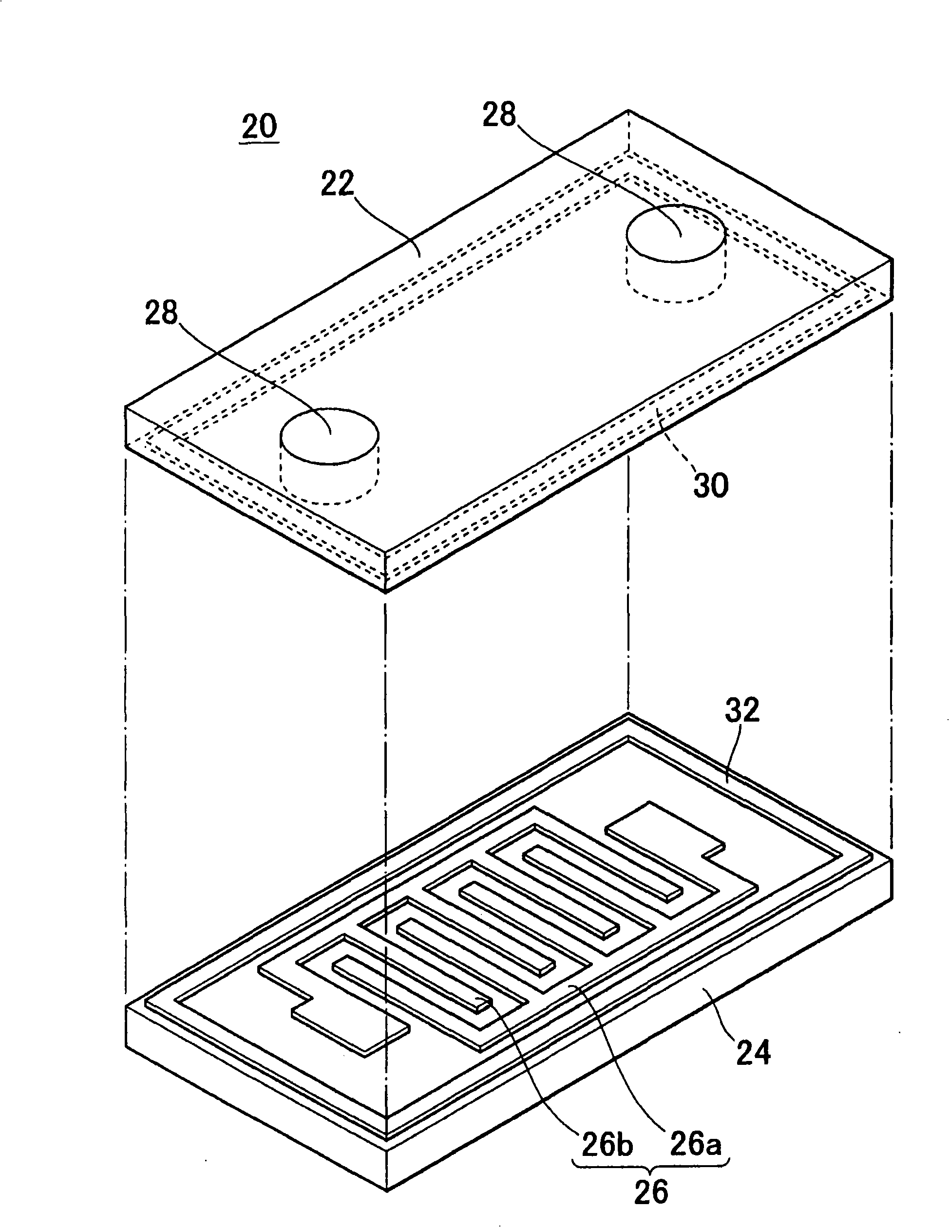
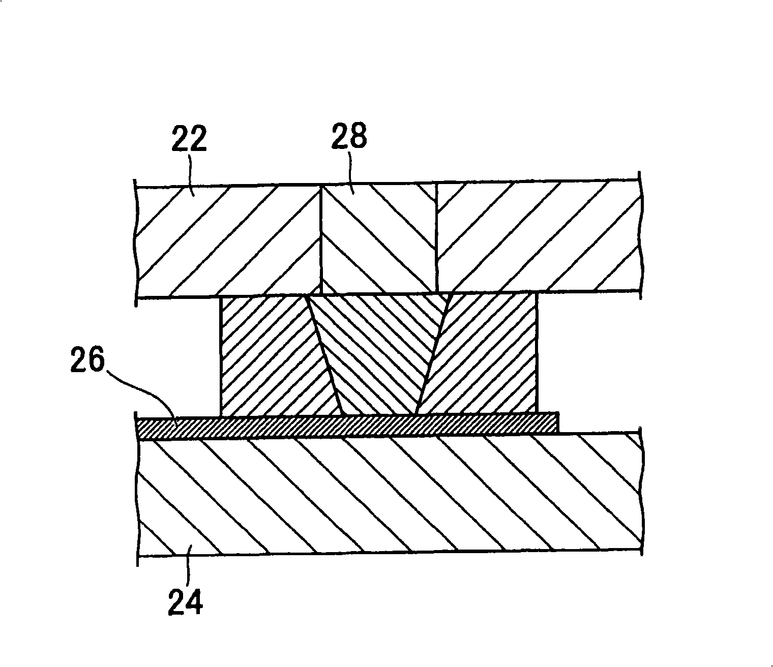
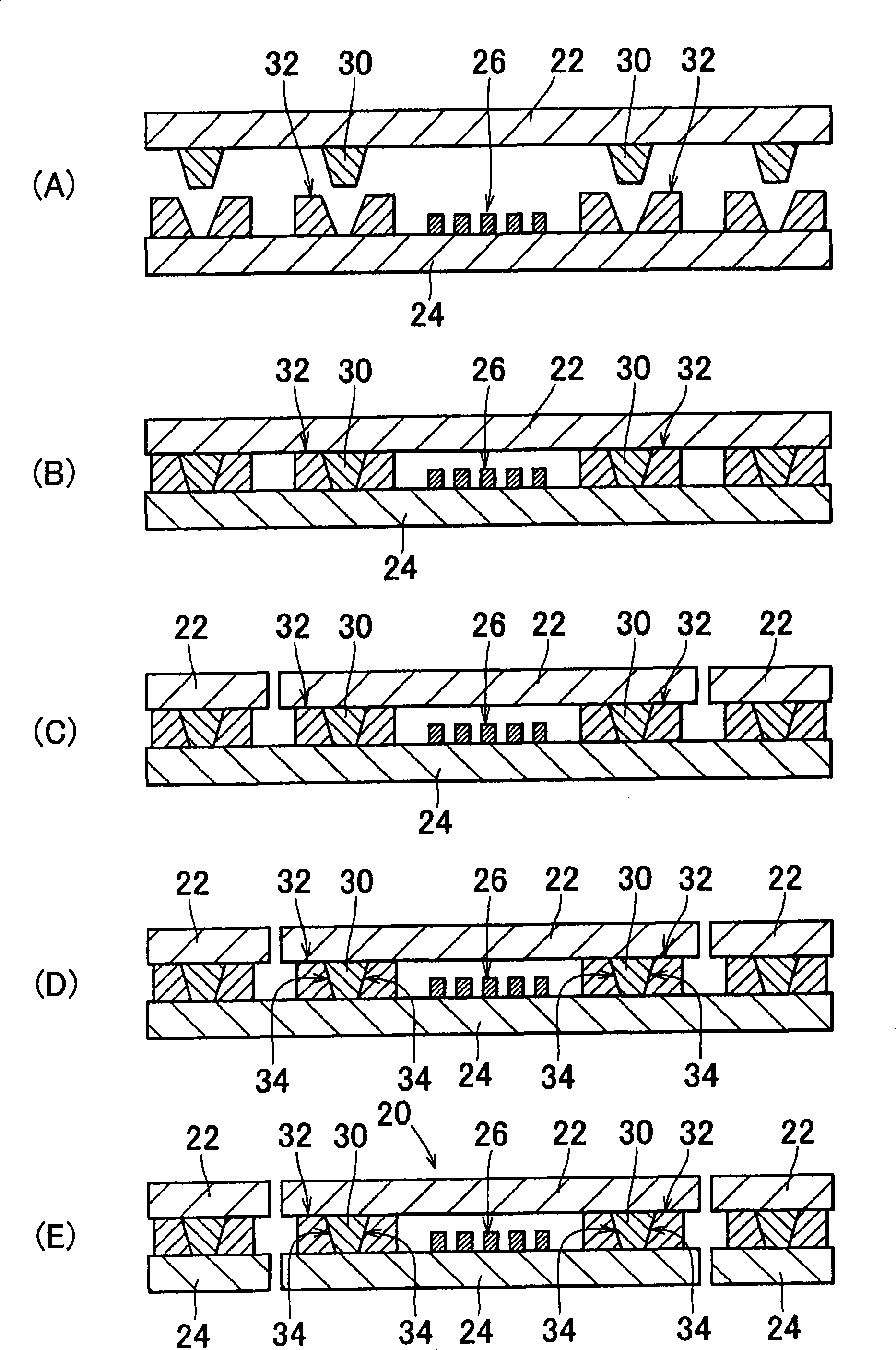
[0058] figure 1 It is an exploded perspective view showing an example of the electronic component of the present invention. Here, as the electronic component 20, an electronic component in which a surface acoustic wave element has been formed will be described, but it may be an electronic component in which another element has been formed. The electronic component 20 includes a first substrate 22 and a second substrate 24. As the first substrate 22 used as a covering member, for example, silicon (Si) is used, and as the second substrate 24 used as a substrate of a surface acoustic wave element, for example, LiTaO is used. 3 And other piezoelectric substrates. Among them, as the material of the first substrate 22 and the second substrate 24, in addition to the above-mentioned materials, LiNbO can also be used according to the formed element or the purpose of the substrate. 3 , Alumina (alumina), SiC, sapphire (sapphire), crystal, Pb (Zr, Ti) O 3 , PbTiO 3 , BaTiO 3 , SrTiO 3 Wait...


PUM


Abstract

There are provided an electronic component in which two substrates are bonded to each other with a large bonding force and a method for manufacturing electronic components in which two substrates can be bonded to each other with a large bonding force and in which the substrates are not likely to be bent and broken. In an embodiment, a plurality of first connection portions 30 is formed on a first substrate 22, and in addition, a plurality of IDT electrodes 26 and a plurality of second connection portions 32 are formed on a second substrate 24. The first connection portions 30 are engaged in concave parts of the second connection portions 32, so that temporary bonding is performed. Between adjacent first connection portions 30, only the first substrate is cut. By heat application, laser irradiation, pressure application, ultrasonic application, or the like, the first connection portions 30 and the second connection portions 32 are finally bonded to each other. The second substrate 24 is cut along the cut portions of the first substrate 22, so that a plurality of electronic components 20 is formed.

Description

technical field [0001] The present invention relates to an electronic component and its manufacturing method, and more particularly, to a chip-shaped electronic component sandwiched between two substrates and its manufacturing method. Background technique [0002] Figure 10 It is a schematic diagram showing the bonding method of two board|substrates used for a conventional electronic component. A first aluminum (Al) film 2 is formed on a first pyrex (registered trademark) glass substrate 1 . In addition, a second aluminum film 4 is formed on a second Pyrex (registered trademark) glass substrate 3 . On the first aluminum film 2 is formed a planar circular and non-tapered concave groove 5 , and on the second aluminum film 4 is formed a planar circular and tapered convex tooth 6 with a tapered front end. These concave grooves 5 are meshed with convex teeth 6, and a compressive load is applied at room temperature, whereby the first substrate 1 and the second substrate 2 are j...

Claims


Application Information

Patent Timeline
IPC IPC(8): H01L23/10H03H9/25
Inventor 藤野博之越户义弘相泽直子山田一上坂健一
Owner MURATA MFG CO LTD
Why Eureka
Try Eureka