Method and system for testing on site programmable gate array

A gate array and test vector technology, applied in the direction of measuring electricity, measuring devices, measuring electrical variables, etc., can solve the problems of consuming FPGA chip test cost, reducing test configuration, and limited application scope, so as to improve fault coverage and improve reliability. Observational, improved measurability effects

Inactive Publication Date: 2009-04-22
无锡引速得科技有限公司
View PDF0 Cites 27 Cited by
  • Summary
  • Abstract
  • Description
  • Claims
  • Application Information

AI Technical Summary

Problems solved by technology

[0007] The ATPG technology that utilizes the scan chain is specifically to adopt a new configurable logic unit (Configurable Logic Block, CLB) structure to make FPGA have intrinsic scanning characteristics, and combined with FPGA timing design FPGA test (Test ofFPGA, TOF) process, simplify the FPGA initial test netlist to speed up the vector generation process and improve the coverage of the generated vectors, and effectively improve the testability of sequential circuits; however, this solution requires more hardware devices and consumes FPGA chips. test cost
[0008] Another type of FPGA test scheme is to use the form of LUT unit and register in the CLB configuration in the test configuration, and detect all interconnection fixed faults and bridge faults by loading the step 0 / 1 test vector, and then The test configuration is reduced to shorten the test time; the specific process is to configure all the look-up tables (Look UpTable, LUT) in the test configuration as AND / OR functions, or single-item functions based on Walsh coding, and load all 0 / 1 vectors or activate Vector can be detected; however, in practical applications, the above scheme uses an assumption in the actual test application, that is, the logic in the FPGA design is only realized by the LUT, which does not meet the actual situation, so the scope of application of the above scheme is limited

Method used


Image

  • Method and system for testing on site programmable gate array
  • Method and system for testing on site programmable gate array
  • Method and system for testing on site programmable gate array

Examples


Embodiment 1

[0075] Such as Figure 4 The flow chart of an FPGA testing method of the present invention is shown; the steps of the FPGA testing method mainly include:

[0076] Step 401: Obtain the initial design netlist and initial design configuration of the field programmable gate array;

[0077] Step 402: Use the exclusive OR function of the logic function to replace the functions of the initial design netlist and the lookup table unit of the initial design configuration to obtain the initial test netlist and the initial test configuration;

[0078] Of course, the exclusive OR function of the logic function mentioned in this step replaces the function of the look-up table unit, that is, as long as any unit configured here has the function of the look-up table unit, the exclusive OR function of the logic function can be used to perform Replacement and replacement are universal, and can be a look-up table unit or a non-look-up table unit. As long as the LUT function is set in the FPGA chip, t...

Embodiment 2

[0114] Another application-oriented FPGA testing method of the present invention has the following steps:

[0115] Step A1: Get the FPGA initial design netlist N containing the LUT configuration D , And initial design configuration, where the FPGA initial design netlist refers to the FPGA initial design netlist obtained after wiring during FPGA design and development;

[0116] Step A2: The FPGA initial design netlist N D The LUT configuration functions in are all modified to XOR logic functions to get the initial test netlist For a LUT, when the input controllability is determined, configuring the LUT as an XOR gate can improve the output controllability;

[0117] Those skilled in the art should know that the controllability and observability of any node involved in the embodiments of the present invention are between 0 and 1. The closer the controllability value of a node is to 1, the higher the controllability of the node, and vice versa. Because the input port is directly cont...

Embodiment 3

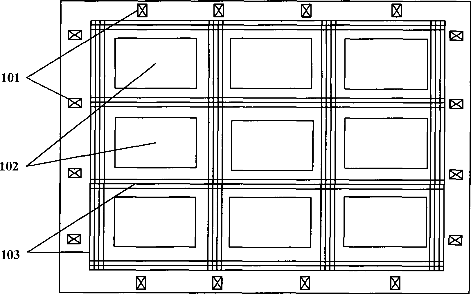
[0138] An application-oriented FPGA test usually uses part of the FPGA resources. The present invention can utilize the reconfigurable characteristics of the FPGA chip to perform application-oriented test analysis, such as image 3 Shown. Can put image 3 The FPGA design configuration example shown is abstracted into Figure 5 The FPGA initial design network example shown. Since there is no scan chain in the FPGA initial design netlist, the testability of its internal nodes is very low, resulting in a low coverage rate of the test vector generated by the automatic test vector generation tool for the netlist.

[0139] In order to improve the testability of the netlist without inserting a scan chain, an FPGA chip that needs to be tested for application is obtained. An example of the test process is as follows:

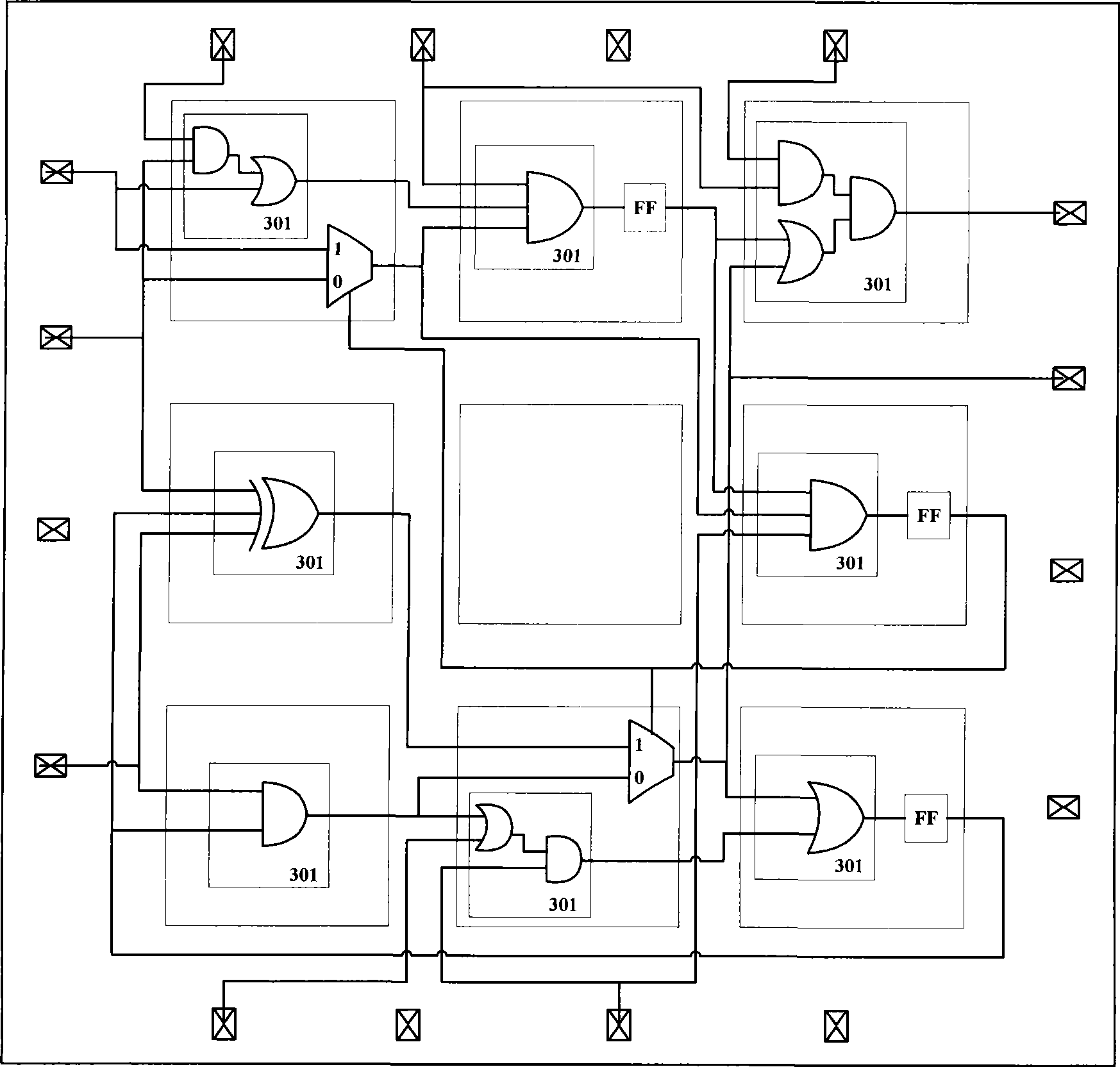
[0140] Step W1: firstly modify all the configuration logic functions 501 of the LUTs into exclusive OR logic functions to improve the controllability of its internal nodes. ...


PUM


Abstract

The invention relates to a testing method for a field programmable gate array (FPGA). The method comprises the following steps: obtaining an initial design netlist and an initial design configuration of the FPGA; replacing a look-up table function of the initial design netlist and the initial design configuration with an exclusive or function of a logic function to obtain an initial testing netlist and an initial testing configuration; selecting an observation node of the initial testing netlist based on a preset rule of a testability analysis method, and obtaining a testing netlist and a corresponding testing vector; configuring an output terminal of an output and input unit from the observation node to the initial testing configuration to obtain a testing configuration; connecting the testing configuration to an configuration device according to an excitation signal of the configuration device to obtain an output logic value of the testing vector; and analyzing the output logic value and a response value of the testing vector to obtain the testing result. The method can effectively detect permanent faults of interconnection lines used in the application design of FPGA chips.

Description

Technical field [0001] The invention relates to a chip testing technology, in particular, to a testing method of a field programmable gate array and a testing system of a field programmable gate array. Background technique [0002] The appearance of Field Programmable Gate Array (FPGA) devices is the result of the development of VLSI technology and computer-aided design technology. FPGA is an erasable programmable read-only memory, usually on a single board. During power-on initialization, load related programs and data to the FPGA hardware chip of the single board; after the FPGA chip is initialized, complex logic control can be completed. [0003] Such as figure 1 As shown, the FPGA structure generally includes three types of basic resources: Input / Output Block (IOB) 101, Configurable Logic Block (CLB) 102, and Interconnect Resources (IR) 103. Among them, IOB can provide a connection interface between FPGA internal logic and package pins, CLB can be used to implement logic and...

Claims


Application Information

Patent Timeline
Patent Type & Authority Applications(China)
IPC IPC(8): G01R31/3185
Inventor 冯建华林腾徐文华王阳元
Owner 无锡引速得科技有限公司
Why Eureka
Try Eureka