PVD chromium based ceramic composite coating piston ring and method for producing the same
A ceramic composite, piston ring technology, applied in the direction of piston ring, coating, metal material coating process, etc., can solve the problems of incapable of large-scale industrial production, reduction of coating growth rate, increase of coating cost, etc. Good prospects for industrial application, good wear resistance and low cost
- Summary
- Abstract
- Description
- Claims
- Application Information
AI Technical Summary
Problems solved by technology
Method used
Image
Examples
Embodiment 1
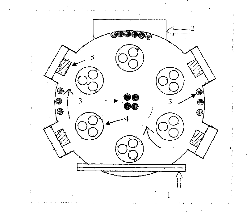
[0018] Example 1: Glow cleaning is performed on the nitriding piston ring at 400°C in an argon environment. During the glow discharge process, the bias voltage on the workpiece is -1000V, and the glow time is 30 minutes; glow cleaning After the end, a transition metal Cr layer with a thickness of 150 nanometers was deposited by arc discharge method under 0.3Pa pressure condition; then 20 micron Cr / CrN main wear-resistant layer was deposited by arc discharge method under 450°C, -150V bias, and 2.3Pa pressure condition. layer, wherein each layer of Cr is 0.2 microns, each layer of CrN is 4.8 microns, the thickness of Cr and CrN two layers is 5 microns, and the main wear-resistant layer includes 4 layers of Cr and 4 layers of CrN; Depositing 10 micron Cr / Cr by arc discharge method at 450°C, -200V bias, and 3.3Pa pressure 2 o 3 Anti-friction layer, wherein each layer of Cr is 0.1 micron, and each layer of Cr 2 o 3 1.9 µm, Cr and Cr 2 o 3 The thickness of the two layers is 2 m...
Embodiment 2
[0019] Example 2: Glow cleaning is performed on the nitriding piston ring at 430°C in an argon environment. During the glow discharge process, the bias voltage on the workpiece is -1200V, and the glow time is 60 minutes; glow cleaning After the end, a transition metal Cr layer with a thickness of 100 nanometers was deposited by arc discharge method at 0.5Pa pressure condition; then 18 micron Cr / CrN main wear-resistant layer was deposited by arc discharge method at 430°C, -200V bias voltage and 3Pa pressure condition , where each layer of Cr is 0.2 microns, each layer of CrN is 4.3 microns, the thickness of the two layers is 4.5 microns, the main wear-resistant layer includes 4 layers of Cr and 4 layers of CrN; when the main wear-resistant layer is deposited, at 450 ° C, - Deposition of 6 micron Cr / Cr by arc discharge under 200V bias and 4.3Pa air pressure 2 o 3 Anti-friction layer, wherein each layer of Cr is 0.2 microns, and each layer of Cr 2 o 3 1.8 µm, Cr and Cr 2 o 3...
Embodiment 3
[0020] Example 3: Glow cleaning the nitriding piston ring at 450°C in an argon environment, the bias voltage on the workpiece during the glow discharge process is -1200V, and the glow time is 30 minutes; glow cleaning After the end, a transition metal Cr layer with a thickness of 150 nanometers was deposited by arc discharge method at 1.0Pa pressure; then a 15 micron Cr / CrN main wear-resistant layer was deposited by arc discharge at 450°C, -230V bias, and 5Pa pressure conditions , wherein each layer of Cr is 0.1 micron, each layer of CrN is 4.9 micron, the thickness of two layers of Cr and CrN is 5 microns, and the main wear-resistant layer includes 3 layers of Cr and 3 layers of CrN; when the main wear-resistant layer is deposited, at 440 Deposit 10 micron Cr / Cr by arc discharge method under the condition of -150V bias voltage and 3.3Pa air pressure 2 o 3 Anti-friction layer, wherein each layer of Cr is 0.1 micron, and each layer of Cr 2 o 3 2.4 microns, Cr and Cr 2 o 3 ...
PUM
| Property | Measurement | Unit |
|---|---|---|
| thickness | aaaaa | aaaaa |
| thickness | aaaaa | aaaaa |
| thickness | aaaaa | aaaaa |
Abstract
Description
Claims
Application Information


