
Solid state semiconductor memory mechanism and its application system and control assembly

A storage device and application system technology, applied in temperature control, static memory, non-electric variable control, etc., can solve the problems of unsuitable solid-state disk drives, solid-state semiconductor storage devices, high heat dissipation, and long-term use

Active Publication Date: 2009-05-13
ADATA
View PDF7 Cites 14 Cited by
  • Summary
  • Abstract
  • Description
  • Claims
  • Application Information

AI Technical Summary

Problems solved by technology

[0009] 3. In terms of power consumption, since it takes a long time for the NADA-type Flash memory to perform memory page write or memory block erase operations, the power consumed by performing this operation is higher than that of simply outputting / inputting data. heat is also higher
[0010] From the above three differences, it can be seen that NADA-type Flash memory and volatile random access memory have different characteristics, so the aforementioned related technologies for memory temperature control cannot be applied to solid-state disk drives or other solid-state semiconductor storage devices.
General solid-state semiconductor storage devices have the problem of unstable operation caused by temperature, so far there is still a lack of better solutions to improve

Method used

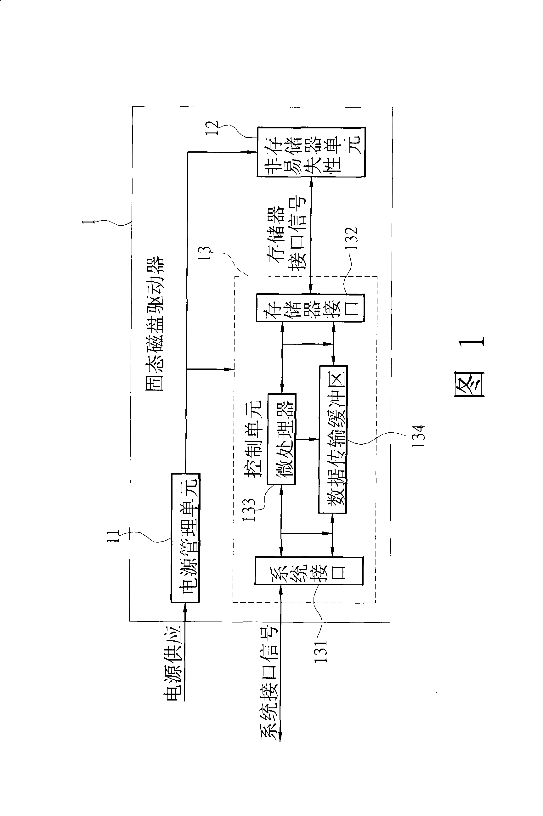
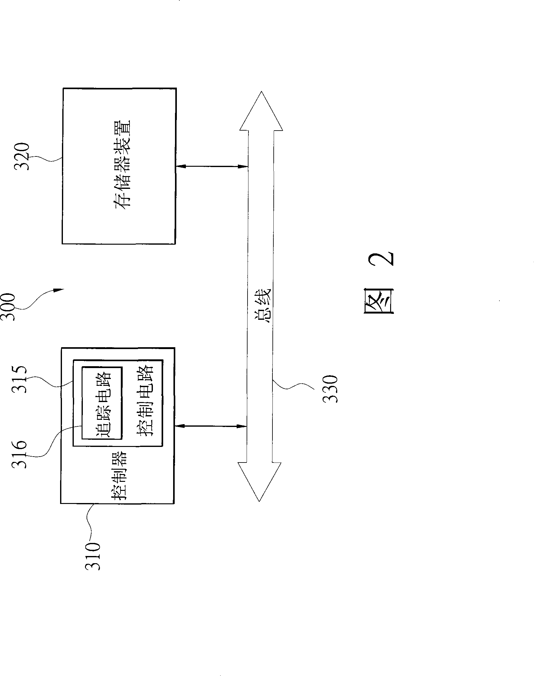
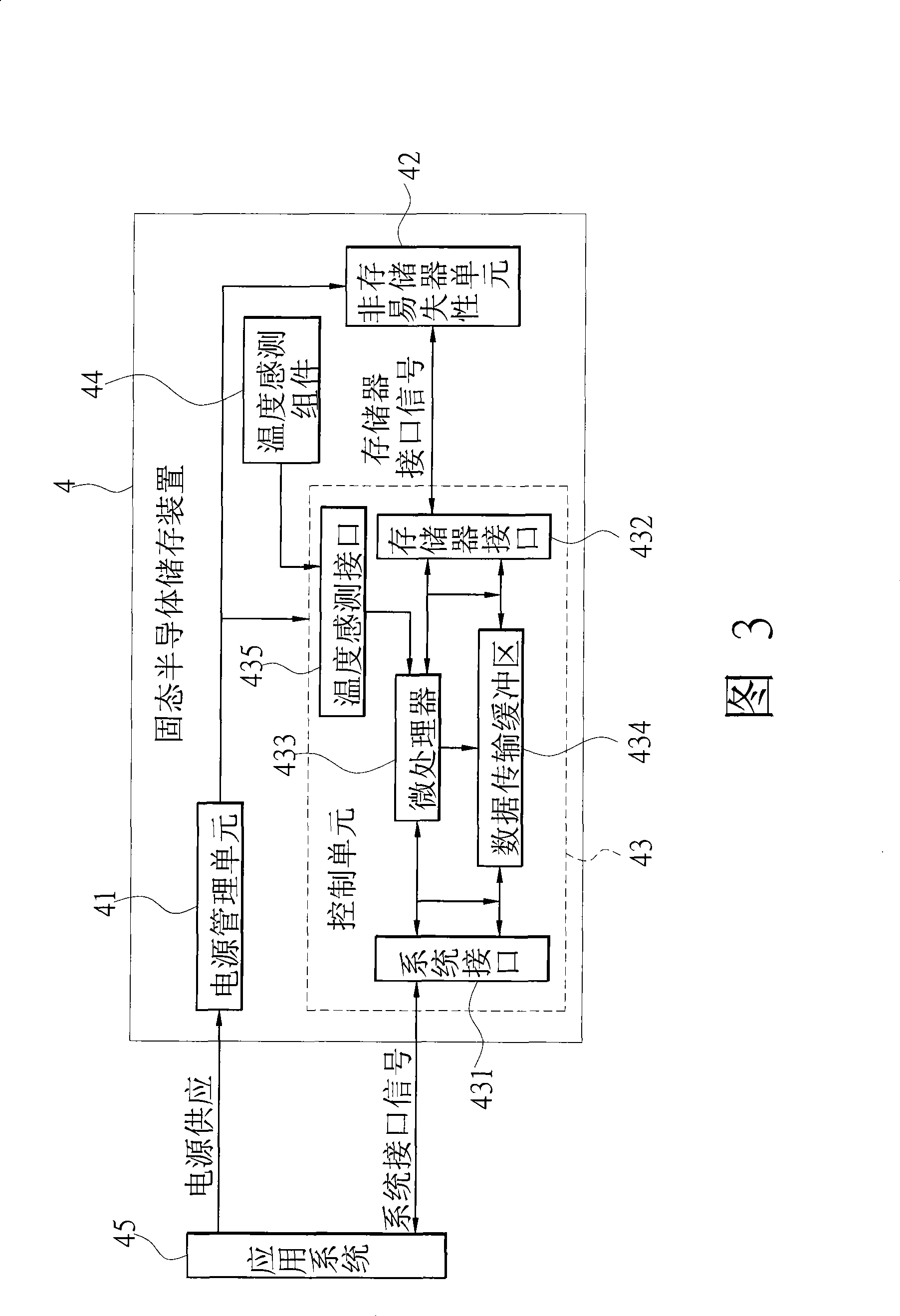

Image

  • Solid state semiconductor memory mechanism and its application system and control assembly
  • Solid state semiconductor memory mechanism and its application system and control assembly
  • Solid state semiconductor memory mechanism and its application system and control assembly

Examples


Embodiment Construction

[0059] Please refer to FIG. 3 , which is a functional block diagram of the solid-state semiconductor storage device with temperature control function of the present invention. As shown in the figure, the solid-state semiconductor storage device 4 with temperature control function includes a power management unit 41 , a non-volatile memory unit 42 , a control unit 43 , and a temperature sensing component 44 . The power management unit 41 receives the power supplied from the motherboard or the application system 45 (such as: computer, personal digital mobile device or various digital multimedia devices), and converts it into a power supply form suitable for each unit inside the solid-state semiconductor storage device 4 . The control unit 43 is connected to the application system 45 via the system interface 431 to receive instructions, and perform data input, data output, storage page writing, storage block erasing and other necessary operations on the non-volatile memory unit 42...


PUM


Abstract

The invention discloses a solid-state semiconductor storage device with a temperature control function, as well as an application system and a control assembly thereof, wherein, the solid-state semiconductor storage device comprises a non-volatile memory cell, a temperature sensing assembly and a control unit. The temperature sensing assembly is used for sensing the operating temperature of the solid-state semiconductor storage device to provide a temperature sensing signal to the control unit, and the control unit judges the operating temperature of the solid-state semiconductor storage device according to a temperature sensing signal value, and performs a corresponding program so as to achieve the purpose of controlling the temperature.

Description

technical field [0001] The invention relates to a solid-state semiconductor storage device of a non-volatile memory, in particular to a solid-state semiconductor storage device with a temperature control function and a control method thereof. Background technique [0002] With the increasing popularity of solid-state semiconductor storage devices, there are many applications for recording and storing digital information using solid-state non-volatile memories, such as USB flash drives, memory cards, and solid-state disk drives (Solid-State Disk drives, SSDs). Among them, the solid-state disk drive with the largest capacity is most suitable for portable computers (such as notebook computers, ultra-mobile PCs (Ultra-mobile PC, UMPC), etc.), so as to replace hard disk drives and provide low power consumption, high storage speed, and high speed. characteristics such as reliability. In order to provide higher storage capacity and access speed, several non-volatile memories need ...

Claims


Application Information

Patent Timeline
IPC IPC(8): G11C7/04G05D23/22
Inventor 陈明达林传生张惠能谢祥安
Owner ADATA
Learn More