

Flash memory
A flash memory and floating gate technology, applied in the direction of electrical components, transistors, electric solid-state devices, etc., can solve problems such as inability to develop smaller sizes, lower component reliability, and limited components
- Summary
- Abstract
- Description
- Claims
- Application Information
AI Technical Summary
Problems solved by technology
Method used
Image

Examples
Embodiment Construction
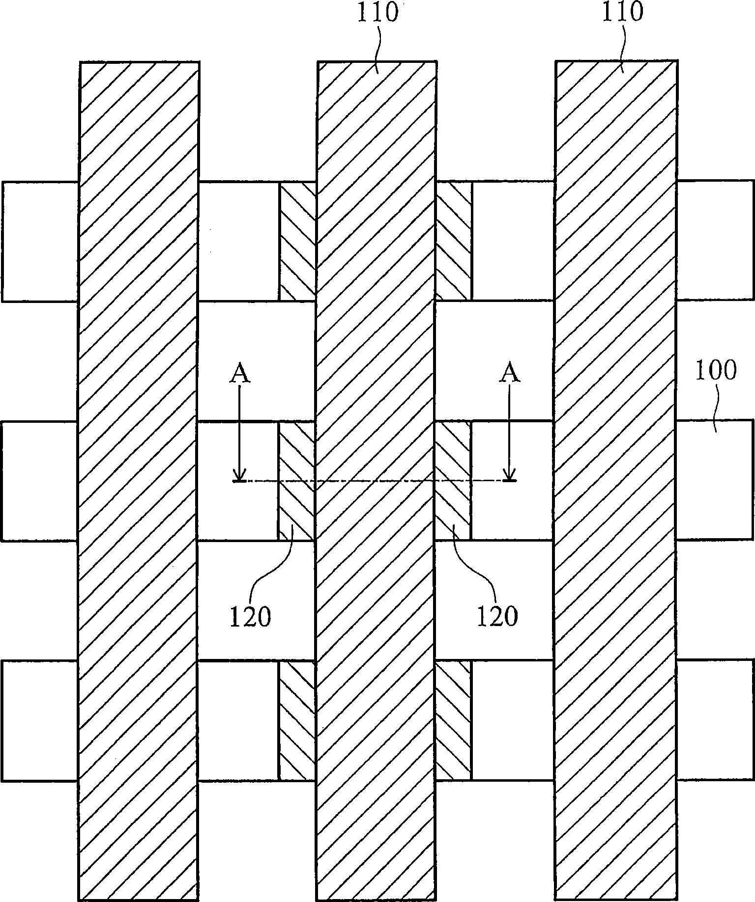
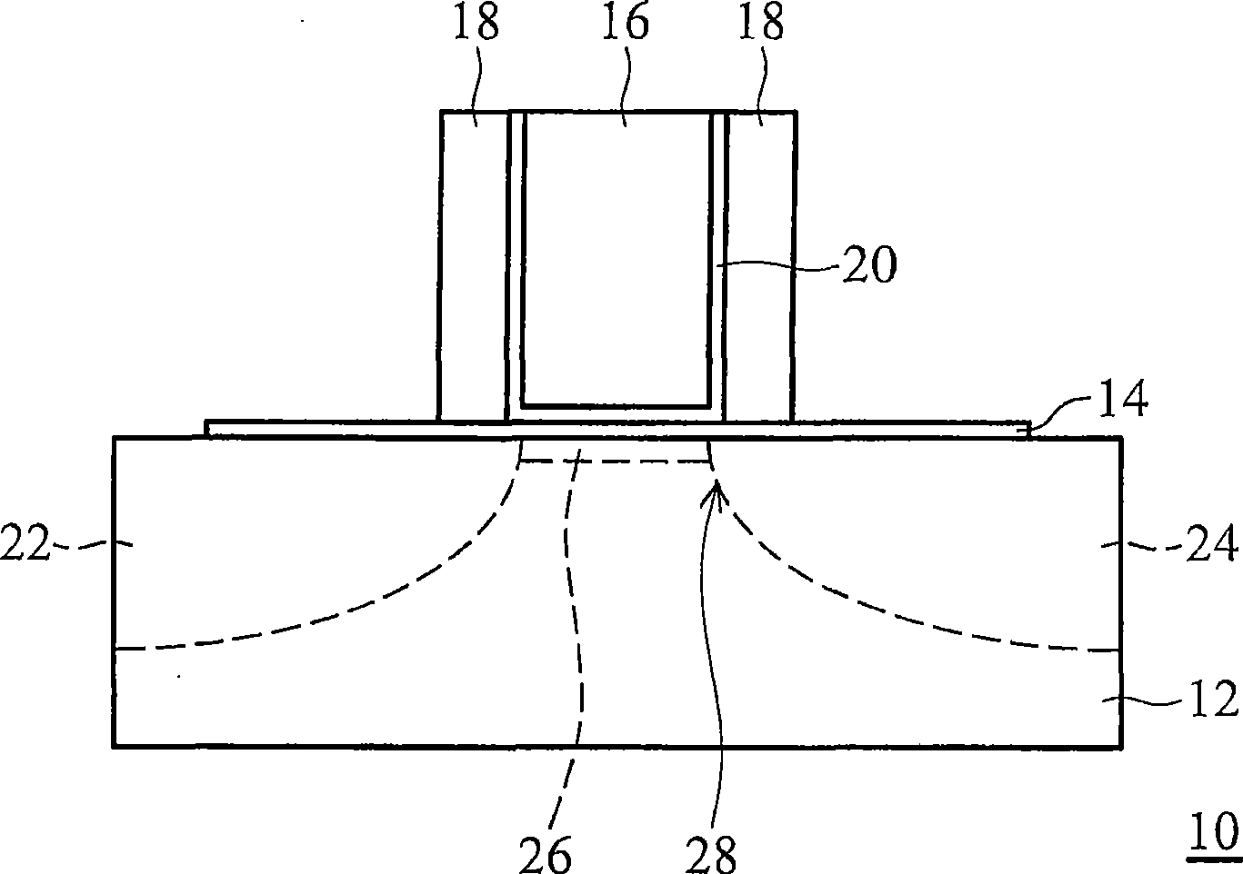
[0028] see Figure 1~2 , illustrating an embodiment of the present invention, a flash memory device. figure 1 It is a plane configuration diagram of a flash memory device. figure 2 for figure 1 A partial cross-sectional schematic view taken along section line A-A.
[0029] figure 1 100 represents an active region, 110 represents a gate layer, and marks 120 on both sides of the gate layer 110 represent two floating gates.
[0030] figure 2 Among them, the flash memory 10 includes a substrate 12 , a first insulating layer 14 , a control gate 16 , two floating gates 18 and a second insulating layer 20 . The first insulating layer 14 is formed on the substrate 12 . The control gate 16 is disposed on the first insulating layer 14 . The two floating gates 18 are respectively coplanar with the substrate 12 and disposed on two sides of the control gate 16 . The second insulating layer 20 is formed between the control gate 16 and the first insulating layer 14 and between the ...
PUM
 Abstract
Description
Claims
Application Information