
On-substrate base sheet micro-processing method

A microfabrication and substrate technology, which is applied in the direction of producing decorative surface effects, microstructure technology, microstructure devices, etc., can solve the problem of not being able to withstand large impacts and overloads, low fracture toughness, and inability to withstand harsh environments. Work and other problems, to achieve the effect of high aspect ratio, high three-dimensional processing

Inactive Publication Date: 2011-05-04
PEKING UNIV
View PDF0 Cites 0 Cited by
  • Summary
  • Abstract
  • Description
  • Claims
  • Application Information

AI Technical Summary

Problems solved by technology

However, the high cost of SOI wafers hinders cost-sensitive applications; in addition, SOI uses silicon as the only structural material, and silicon materials have disadvantages such as poor electrical conductivity and low fracture toughness, which restrict the performance and application of devices. Range and reliability, such as applications that require contact conduction need to use a special process to form sidewall coverage on the silicon surface, and long-term work will cause contact failure (Aharon, O., Feldman, S., Nemirovsky, Y., Vertically integrated silicon single crystalline MEMS switch, Solid-State Sensors, Actuators and Microsystems, 2005. Digest of Technical Papers. TRANSDUCERS′05. The 13th International Conference on, Page(s): 1047-1050 Vol.1)
In addition, silicon materials are brittle, not resistant to large shocks and large overloads, and cannot work in harsh environments, which limits the application range of devices

Method used


Image

  • On-substrate base sheet micro-processing method
  • On-substrate base sheet micro-processing method
  • On-substrate base sheet micro-processing method

Examples


Embodiment 1

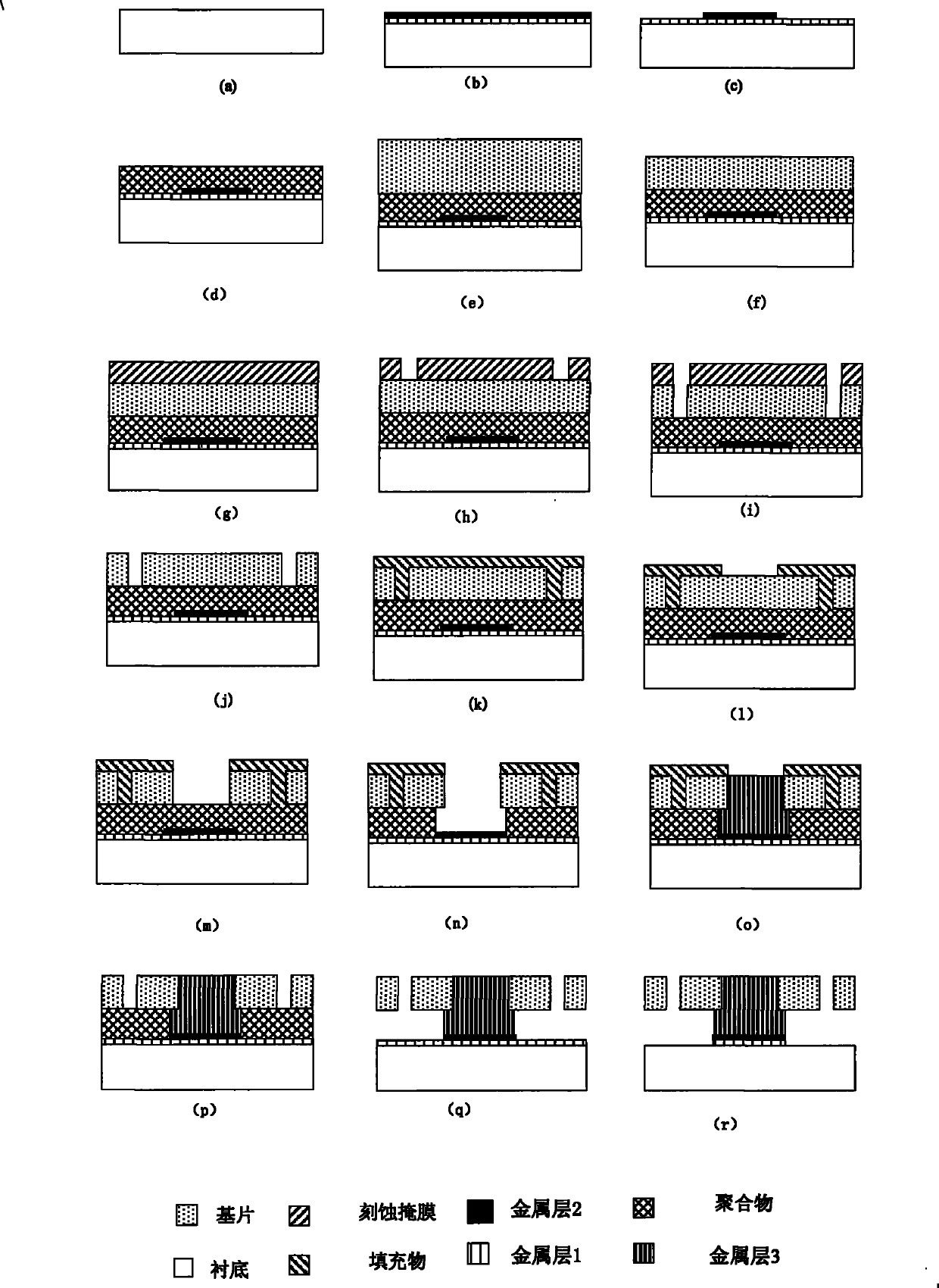
[0029] Embodiment 1, the method of preparing plated holes after first etching through holes is adopted, and the specific steps are:

[0030] 1. Substrate preparation: glass, silicon, metal titanium, aluminum or molybdenum can be used as the substrate, see figure 1 (a).

[0031] 2. Selection of substrate: The substrate material can be silicon, germanium, III-V compound, metal titanium, aluminum or molybdenum, etc.

[0032] 3. Metal or metal compound layer 1 and layer 2 are deposited on the surface of the substrate, and the metal layer 2 is patterned.

[0033] Specifically, in order to ensure that the subsequent electroplating only occurs in the area of ​​the metal layer 2, first deposit a metal layer 1 that does not undergo electroplating on the surface of the substrate, such as sputtering Cr 30nm; then deposit a metal layer 2, such as sputtering Au 500nm ;,like figure 1 As shown in (b), metal layer 2 is patterned, see figure 1 (c).

[0034] 4. The polymer is used as an in...

Embodiment 2

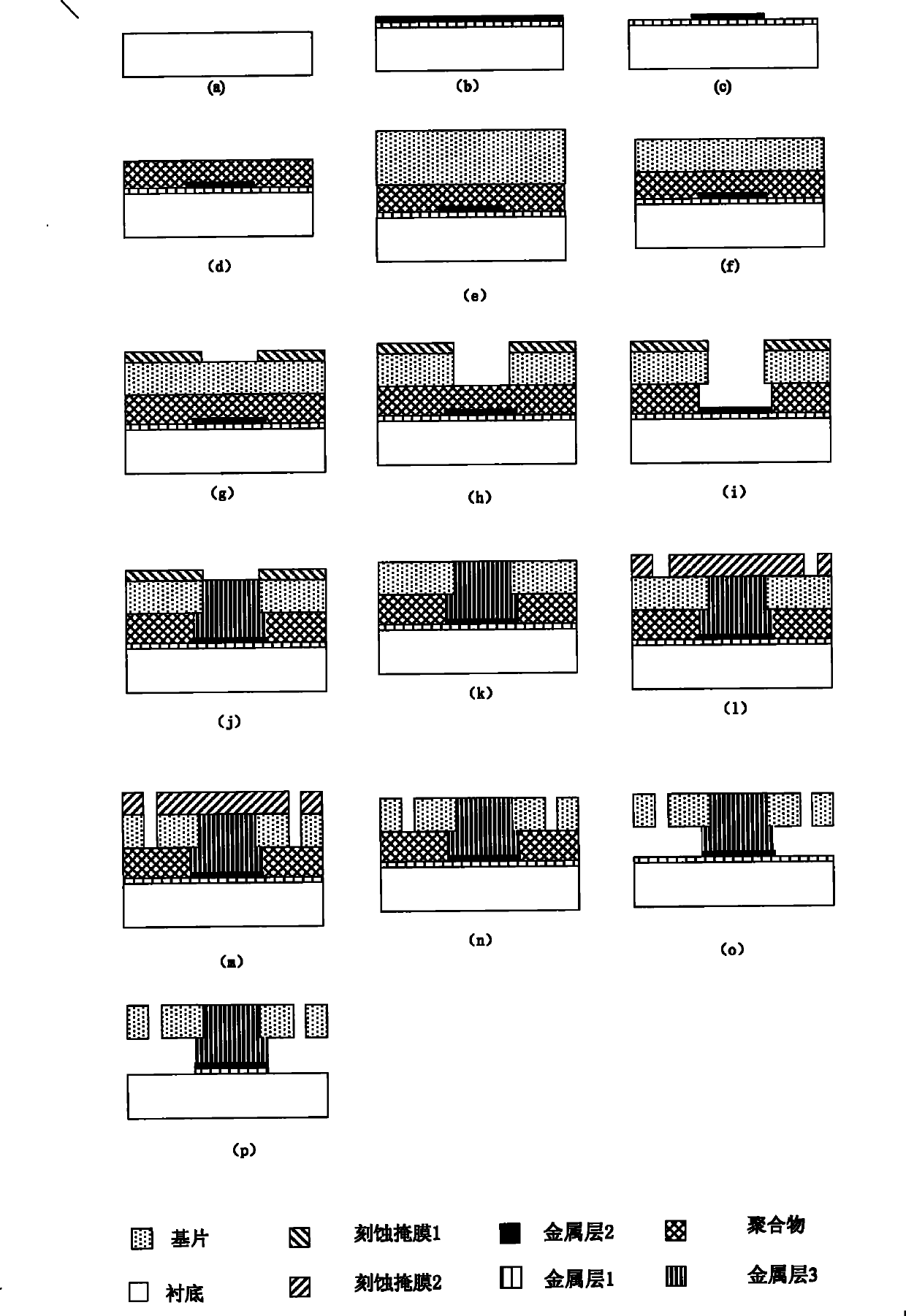
[0048] Embodiment 2, the method of etching the through hole after preparing the plated hole first, the specific steps are:

[0049] 1. Preparation of the substrate: glass, silicon, metal titanium, aluminum or molybdenum can be used as the substrate, such as figure 2 (a) shown.

[0050] 2. Selection of substrate: The substrate material can be silicon, germanium, III-V compound, metal titanium, aluminum or molybdenum, etc.

[0051] 3. Metal or metal compound layer 1 and layer 2 are deposited on the surface of the substrate, and the metal layer 2 is patterned.

[0052] Specifically, in order to ensure that the subsequent electroplating only occurs in the area of ​​the metal layer 2, first deposit a metal layer 1 that does not undergo electroplating on the surface of the substrate, such as sputtering Cr 30nm; then deposit a metal layer 2, such as sputtering Au 500nm ,like figure 2 Shown in (b); metal layer 2 is patterned, see figure 2 (c).

[0053] 4. The polymer is used a...


PUM


Abstract

The invention discloses an on-substrate base sheet micro-processing method. The method comprises the following steps: bonding a substrate with a base sheet by using a polymer as the intermediate adhesion layer by pressure bonding to form an on-substrate base sheet; thinning the base sheet and deeply etching to form a through hole; back-filling the through hole, and deeply etching the base sheet to form an electroplating hole; electroplating metal in the electroplating hole to form a support between the substrate and the base sheet; and releasing the through hole, etching the polymer through the through hole so as to release the structure. Alternatively, the method comprises the steps of thinning the base sheet after forming the on-substrate base sheet and deeply etching to form an electroplating hole; electroplating metal in the electroplating hole to form a support between the substrate and the base sheet; deeply etching the base sheet to form a through hole; etching the polymer through the through hole; and releasing the structure. The method can achieve low-cost, high-accuracy and high-aspect-ratio 3D processing of a plurality kinds of materials, and the micromachining process compatible to the CMOS process can be used for processing a plurality kinds of MEMS devices.

Description

technical field [0001] The invention relates to micro-processing technology of micro-electro-mechanical system (MEMS), in particular to a micro-processing method of a substrate on a substrate. Background technique [0002] At present, SOI (silicon on insulator) technology is playing an increasingly important role in the fields of semiconductors and micromechanics. SOI MEMS devices with high aspect ratio are applied to inertial sensors and electrostatic drives. The obtained devices have simple process, high efficiency, large capacitor plate area, large driving force, small chip area occupied, high power carrying capacity and high integration (Siavash Pourkamali, and Farrokh Ayazi, SOI-Based HF And VHF Single-Crystal Silicon Resonators With Sub-100Nanometer Vertical Capacitive Gap, Transducers'03, pp.837-840.). However, the high cost of SOI wafers hinders cost-sensitive applications; in addition, SOI uses silicon as the only structural material, and silicon materials have sho...

Claims


Application Information

Patent Timeline
Patent Type & Authority Patents(China)
IPC IPC(8): B81C1/00
CPCB81C1/00039B81C2201/0108
Inventor 陈兢张轶铭
Owner PEKING UNIV
Learn More