Surface treatment copper foil and surface treatment method as well as laminated circuit basal board

A surface treatment layer and surface treatment technology, applied in the direction of circuit substrate materials, printed circuit components, chemical instruments and methods, etc., can solve the problems of improving the bonding strength between copper foil and polyimide, and achieve the effect of high bonding strength

Active Publication Date: 2011-04-27
FURUKAWA ELECTRIC CO LTD
View PDF2 Cites 0 Cited by
  • Summary
  • Abstract
  • Description
  • Claims
  • Application Information

AI Technical Summary

Problems solved by technology

[0005] In this bonding process at high temperature, there is a problem of improvement of bonding strength between copper foil and polyimide at high temperature.

Method used


Image

  • Surface treatment copper foil and surface treatment method as well as laminated circuit basal board
  • Surface treatment copper foil and surface treatment method as well as laminated circuit basal board
  • Surface treatment copper foil and surface treatment method as well as laminated circuit basal board

Examples


Embodiment 1、2

[0039] Add NaH under the conditions to achieve 0.6g / L in terms of P metal content 2 PO 2 ·H 2 o

[0040] Add ZnSO under the condition of 0.5g / L in terms of Zn metal component 4 ·7H 2 o

[0041] As other ingredients, add 1.0g / L H 3 BO 3

[0042] Bath temperature: 45°C

[0043] pH: 3.5

[0044] Current density: 0.5A / dm 2

[0045] Processing time: 10 seconds

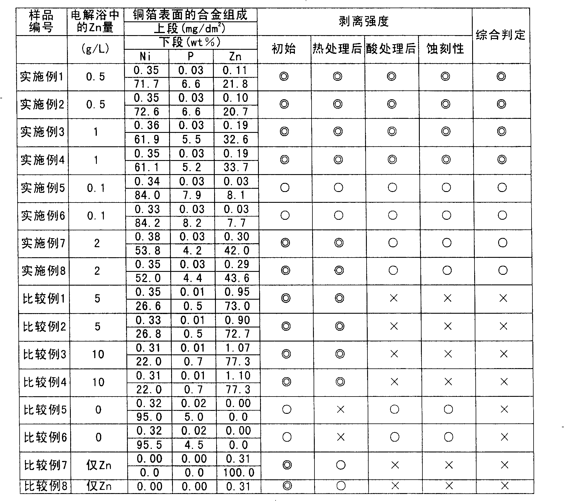
[0046] Surface treatment was performed twice on the above-mentioned untreated copper foil with the electrolytic bath of the above-mentioned composition and its conditions. As Example 1 for the first time and Example 2 for the second time, the following measurements were performed on the surface-treated copper foil, and the measurement results are shown in Table 1 as Examples 1 and 2.

[0047] (1) Alloy composition of the surface treatment layer deposited on the surface of the copper foil: analyzed by fluorescent X-rays.

[0048] (2) Initial peel strength: The surface-treated copper foil in Examples 1 and 2 was b...

Embodiment 3、4

[0055] Add NaH under the conditions to achieve 0.6g / L in terms of P metal content 2 PO 2 ·H 2 o

[0056] Add ZnSO under the condition of 1.0g / L in terms of Zn metal component 4 ·7H 2 o

[0057] As other ingredients, add 1.0g / L H 3 BO 3

[0058] Bath temperature: 45°C

[0059] pH: 3.5

[0060] Current density: 0.5A / dm 2

[0061] Processing time: 15 seconds

[0062] Surface treatment was performed twice on the above-mentioned untreated copper foil with the electrolytic bath of the above-mentioned composition and its conditions. The same measurement as Example 1 was performed about the surface-treated copper foil, and the first time was made into Example 3, and the second time was made into Example 4, and the results are shown in Table 1 as Examples 3 and 4.

[0063]

[0064] Copper foil (untreated copper foil): WZ copper foil of Furukawa Circuit Copper Foil Co., Ltd., Rz: 1.0

Embodiment 5、6

[0066] Add NaH under the conditions to achieve 0.6g / L in terms of P metal content 2 PO 2 ·H 2 o

[0067] Add ZnSO under the condition of 0.1g / L in terms of Zn metal component 4 ·7H 2 o

[0068] As other ingredients, add 1.0g / L H 3 BO 3

[0069] Bath temperature: 45°C

[0070] pH: 3.5

[0071] Current density: 0.5A / dm 2

[0072] Processing time: 4 seconds

[0073] Surface treatment was performed twice on the above-mentioned untreated copper foil with the electrolytic bath of the above-mentioned composition and its conditions. The same measurement as in Example 1 was performed on the surface-treated copper foil, and the first time was taken as Example 5, and the second time was taken as Example 6. The results are shown in Table 1 as Examples 5 and 6.

[0074]

[0075] Copper foil (untreated copper foil): WZ copper foil of Furukawa Circuit Copper Foil Co., Ltd., Rz: 1.0


PUM

PropertyMeasurementUnit
peel strengthaaaaaaaaaa

Abstract

The present invention provides a surface treatment copper foil capable of overall satisfying bond strength, acid resistance and etching performance with polyimide, a sureface treatment method for the surface treatment copper foil and a laminated circuit basal board using the surface treatment copper foil. The surface treatment copper foil is formed by applying a surface treatment layer made of Ni-P-Zn alloy on at least one surface of a copper foil. The surface treatment method of the copper foil is that a surface treatment layer is formed by Ni-P-Zn alloy formed by electrobath containing Ni of 0.1 to 200 g / L, P: 0.01 to 50 g / L, Zn of 0.01 to 100 g / L on at least one surface of a non treatment copper foil. The laminated circuit basal board is formed by joining a resin basal board with a surface with the surface treatment layer of the surface treatment copper foil.

Description

technical field [0001] The present invention relates to a surface-treated copper foil, and more particularly to a surface-treated copper foil capable of forming a precise circuit as a laminated circuit board used for high-temperature bonding with polyimide, a surface treatment method thereof, and a laminated circuit board using the copper foil. Background technique [0002] When the copper foil for a printed wiring board is bonded to a resin substrate, it is necessary to improve the bonding strength and to satisfy electrical characteristics, etching characteristics, heat resistance, and chemical resistance required for a printed wiring board. Therefore, the following various treatments are performed: roughening the bonding surface of the copper foil after foil production (hereinafter also referred to as untreated copper foil) and the resin substrate, and then performing plating on the roughened surface. Zinc (Zn) or nickel (Ni) plating, etc., and chromate treatment or the li...

Claims


Application Information

Patent Timeline
Patent Type & Authority Patents(China)
IPC IPC(8): C25D3/56C25D7/06H05K1/09H05K3/38
CPCB32B15/01B32B15/08B32B15/20B32B37/06B32B2311/12B32B2311/20B32B2311/22B32B2457/08H05K1/03
Inventor 藤泽哲铃木裕二
Owner FURUKAWA ELECTRIC CO LTD
Why Eureka
Try Eureka