Manufacturing method for STI isolation structure

An isolation structure and wet etching technology, which is applied in semiconductor/solid-state device manufacturing, electrical components, circuits, etc., can solve problems such as film residue, STI structure corner shape is steep, and affects device chip circuit characteristics, etc., to achieve corrosion The effect of fast speed and avoiding side wall problems

Active Publication Date: 2009-06-10
SHANGHAI HUAHONG GRACE SEMICON MFG CORP
View PDF0 Cites 3 Cited by
  • Summary
  • Abstract
  • Description
  • Claims
  • Application Information

AI Technical Summary

Problems solved by technology

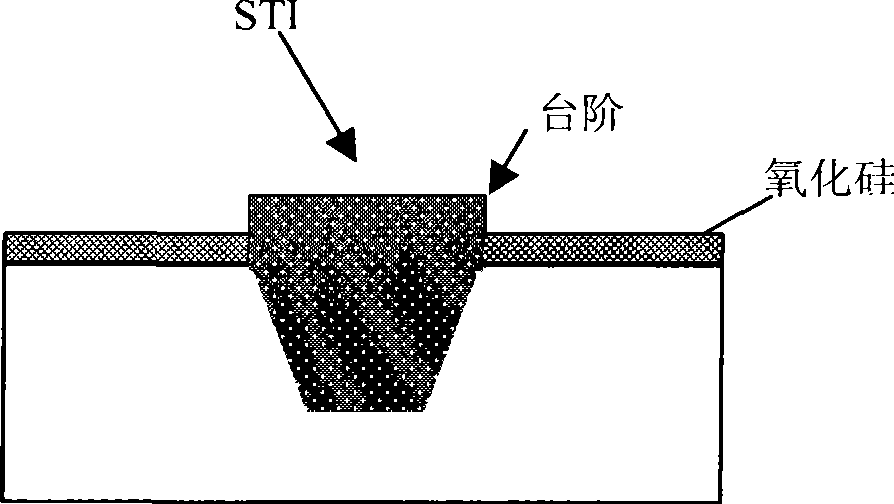
In the 0.13um EFlash process, various regional densities and doping differences lead to too high steps formed by silicon oxide on the isolation region of some regions, and the corners of the STI structure are steep. Sometimes there are film residues on the sidewalls of the steps (for example, etching silicon nitride will form silicon nitride sidewalls at the corners to make silicon nitride residues), which will affect the circuit characteristics of the device and the entire chip

Method used


Image

  • Manufacturing method for STI isolation structure
  • Manufacturing method for STI isolation structure
  • Manufacturing method for STI isolation structure

Examples


Embodiment Construction

[0012] STI structure preparation method flow process of the present invention is:

[0013] (1) A pad oxide layer is grown on the substrate silicon, and then a hard mask layer (usually silicon nitride) is deposited. The function of the hard mask layer is to protect the silicon that does not need to be etched in the subsequent etching process. part;

[0014] (2) Photoresist coating and exposure development to define the position of the shallow groove;

[0015] (3) Hard mask layer etching and photoresist removal, the exposed hard mask layer is partially etched away, and a dry etching process can be used, and then the photoresist is removed;

[0016] (4) dry etching silicon, forming shallow grooves on the substrate silicon, and the etching process can be plasma etching;

[0017] (5) Thermally grow an oxide layer inside the groove, the purpose of which is to repair the surface of the groove damaged during the etching process, and the thickness of the oxide layer is the same as th...


PUM


Abstract

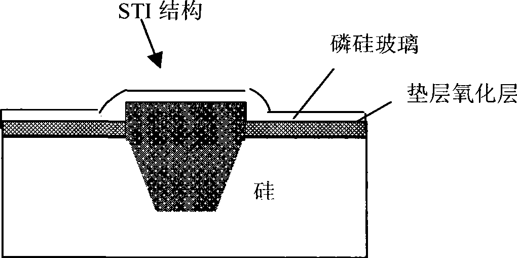
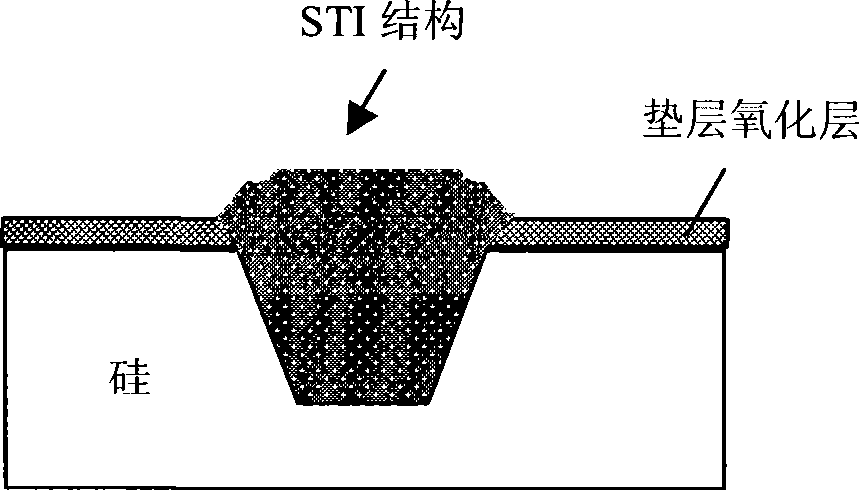
The invention discloses a method for preparing an STI isolation structure. After completing a filling of a shallow groove and removing a hard mask, the method also comprises the following steps: depositing one layer of phosphor on the surface of an oxide layer of a cushion layer; diffusing the phosphor on the surface of the oxide layer of the cushion layer to form phosphorosilicate glass while depositing; and eroding the phosphorosilicate glass through a wet method. The preparation method utilizes the phosphor doping distribution to decide the corrosion speed of each region, finally carries out rounding treatment on corners of the STI structure and is suitable for manufacturing an integrated circuit.

Description

technical field [0001] The invention relates to a preparation method in the manufacture of semiconductor chips, in particular to a preparation method of an STI isolation structure. Background technique [0002] The STI isolation structure (that is, the shallow trench isolation structure) is an isolation structure commonly used in small sizes at present. In the 0.13um EFlash process, various regional densities and doping differences lead to too high steps formed by silicon oxide on the isolation region of some regions, and the corners of the STI structure are steep. Sometimes there are film residues on the sidewalls of the steps (for example, etching silicon nitride will form silicon nitride sidewalls at the corners to make silicon nitride residues), which will affect the circuit characteristics of the device and the entire chip. Contents of the invention [0003] The technical problem to be solved by the present invention is to provide a method for preparing an STI isolat...

Claims


Application Information

Patent Timeline
Patent Type & Authority Applications(China)
IPC IPC(8): H01L21/762H01L21/311
Inventor 陈广龙龚新军
Owner SHANGHAI HUAHONG GRACE SEMICON MFG CORP
Why Eureka
Try Eureka