Chemical mechanical polishing method

A chemical-mechanical, dielectric layer technology, used in grinding devices, grinding machine tools, grinding/polishing equipment, etc., can solve problems such as short circuits, inability to be completely removed, affecting structural thickness and flatness, etc.

Inactive Publication Date: 2009-06-17
SEMICON MFG INT (SHANGHAI) CORP
View PDF1 Cites 4 Cited by
  • Summary
  • Abstract
  • Description
  • Claims
  • Application Information

AI Technical Summary

Problems solved by technology

Erosion occurs in the dense array area of ​​narrow wires, causing over-grinding of oxides between copper metal wires and wires, affecting the thickness and flatness of the entire structure, such as Figure 1B The copper metal wire 11 and the abrasion 11a on the oxide 12 are shown
Both dishing and abrasion lead to thinner wires and higher resistance, and when the dielectric layer and metal layer are formed on top of the dishing or abrasion metal layer, the deposition of oxide will cause a pit that accumulates in the The copper metal in this cavity may not be completely removed during the subsequent chemical mechanical polishing process, which will cause a short circuit in this layer

Method used


Image

  • Chemical mechanical polishing method
  • Chemical mechanical polishing method
  • Chemical mechanical polishing method

Examples


Embodiment Construction

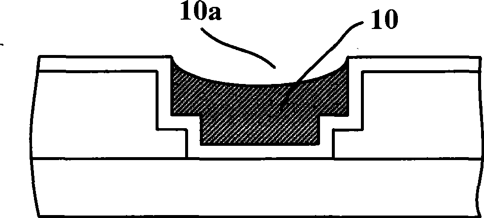
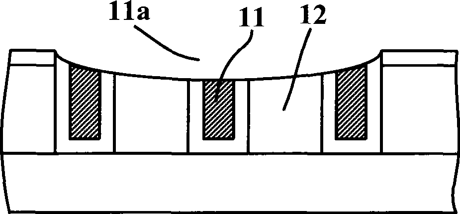
[0031] In the embodiment of the present invention, after grinding and removing most of the copper metal outside the opening of the dielectric layer of the semiconductor substrate, an inhibitor for delaying the copper grinding rate is added to continue grinding the semiconductor substrate to remove the remaining copper metal outside the opening. The dishing of the copper metal is also reduced because the copper metal grinds at a lower rate so that the copper grinds at a rate similar to that of its surrounding material.

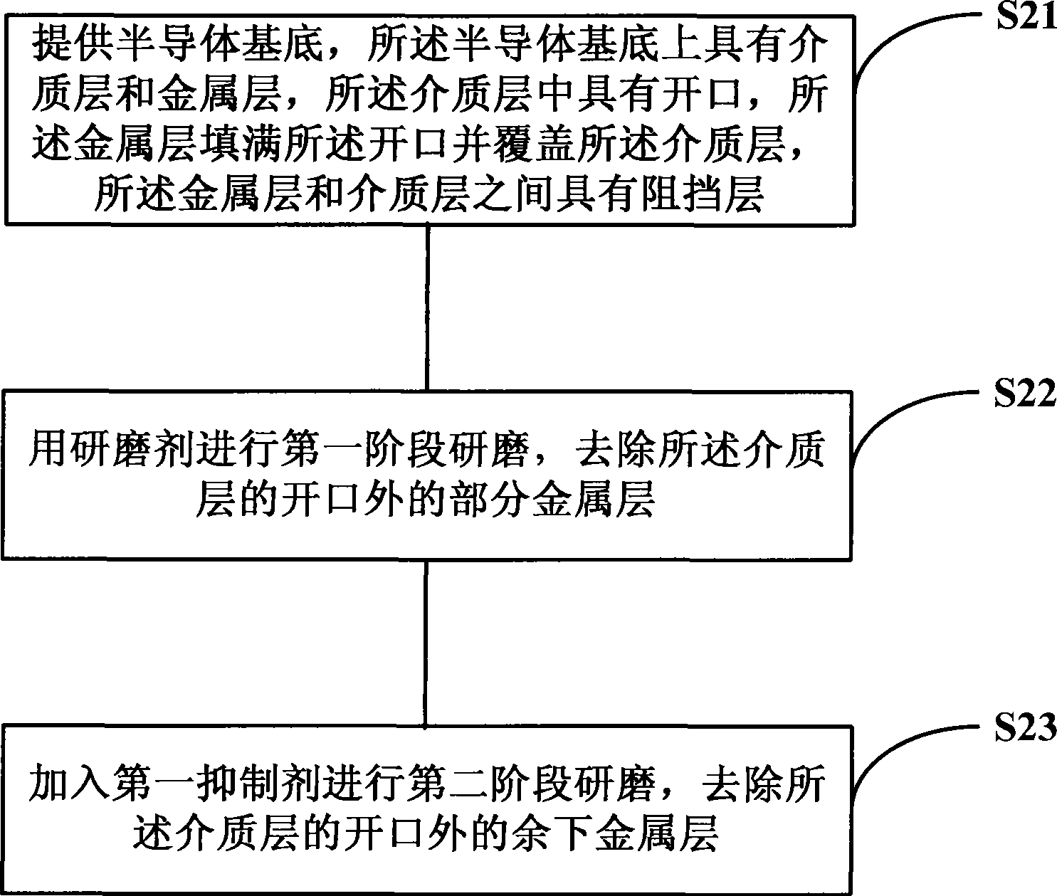
[0032] The basic process of the method of chemical mechanical polishing in the embodiment of the present invention is as follows figure 2 shown, including the following steps:

[0033] Step S21, providing a semiconductor substrate, the semiconductor substrate has a dielectric layer and a metal layer, the dielectric layer has an opening, the metal layer fills the opening and covers the dielectric layer, the metal layer and the dielectric layer There is a barri...


PUM


Abstract

The invention relates to a method for chemico-mechanical grinding. The method comprises the following steps: providing a semiconductor substrate which is provided with a medium layer and a metal layer, wherein the medium layer is provided with an opening, the metal layer fully fills the opening and covers the medium layer, and a barrier layer is arranged between the metal layer and the medium layer; performing the first stage of grinding by using a grinding agent to remove part of the metal layer outside the opening of the medium layer; and performing the second stage of the grinding by adding a first inhibitor to remove the remaining metal layer outside the opening of the medium layer. The method for chemico-mechanical grinding can reduce disk-shaped deboss and abrasive erosion caused in the grinding process.

Description

technical field [0001] The invention relates to the technical field of semiconductor manufacturing, in particular to a chemical mechanical polishing method. Background technique [0002] Chemical Mechanical Polishing (CMP, Chemical Mechanical Polishing) is the use of corrosive abrasives (Slurry) and polishing pads (Pad) in conjunction with mechanical polishing to remove the excess metal layer (metal layer) on the surface of the semiconductor substrate and any surrounding materials. (for example, oxide dielectric layer (oxide layer), barrier layer), and smooth the surface of the semiconductor substrate to achieve comprehensive planarization, reduce design layout restrictions, increase wiring density, reduce defect density, and improve process yield. [0003] The Chinese invention patent application with the application number 200510099539.8 discloses a method of chemical mechanical polishing, including: providing a semiconductor substrate with an opening, a copper metal layer...

Claims


Application Information

Patent Timeline
Patent Type & Authority Applications(China)
IPC IPC(8): B24B29/00B24B37/04H01L21/304
Inventor 李福洪李艳红
Owner SEMICON MFG INT (SHANGHAI) CORP
Why Eureka
Try Eureka