Polishing method of TSV

A technology of through-silicon vias and copper layers, applied in semiconductor devices, electrical components, circuits, etc., can solve problems affecting the electrical properties of devices, achieve the effects of eliminating dent defects, reducing grinding rates, and improving electrical properties

Active Publication Date: 2019-12-27
SEMICON MFG INT (SHANGHAI) CORP
View PDF6 Cites 0 Cited by
  • Summary
  • Abstract
  • Description
  • Claims
  • Application Information

AI Technical Summary

Problems solved by technology

However, due to the large aspect ratio of TSV, after the copper electroplating process, a filling ring will appear on the copper surface above the through hole, such as figure 1 As shown, the semiconductor substrate 100 has a TSV 110, the semiconductor substrate 100 is covered with a copper layer 200, the copper layer 200 fills the TSV 110, and the copper surface above the copper layer 200 will be having a filled ring 210, figure 2 It is a scanned electronic picture of the filled ring 210, after the CMP process, the position of the filled ring will appear as follows image 3 The dent defect shown, which affects the electrical performance of the device

Method used


Image

  • Polishing method of TSV
  • Polishing method of TSV
  • Polishing method of TSV

Examples


Embodiment Construction

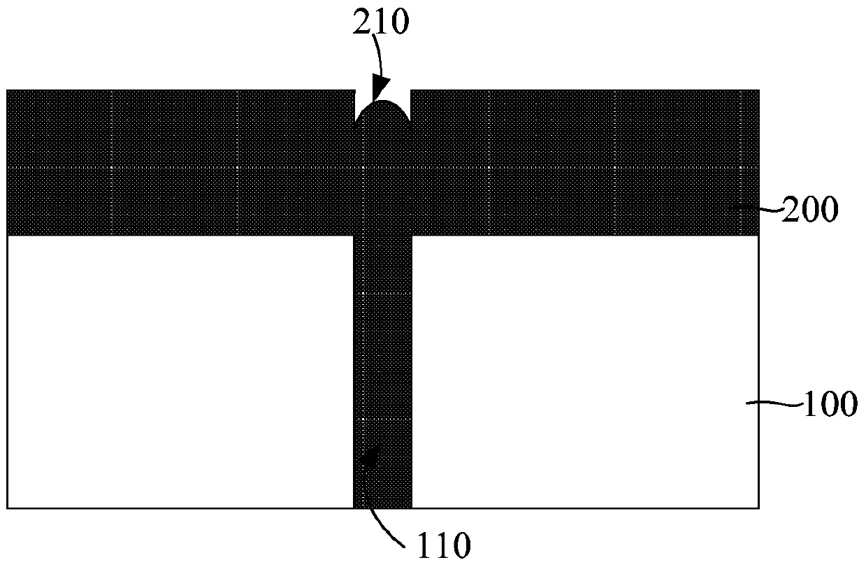
[0033] The method for polishing TSVs of the present invention will be described in more detail below in conjunction with schematic diagrams, wherein a preferred embodiment of the present invention is shown, and it should be understood that those skilled in the art can modify the present invention described here and still realize the present invention beneficial effect. Therefore, the following description should be understood as the broad knowledge of those skilled in the art, but not as a limitation of the present invention.

[0034] In the interest of clarity, not all features of an actual implementation are described. In the following description, well-known functions and constructions are not described in detail since they would obscure the invention with unnecessary detail. It should be appreciated that in the development of any actual embodiment, numerous implementation details must be worked out to achieve the developer's specific goals, such as changing from one embod...


PUM


Abstract

The invention discloses a through-silicon via polishing method which comprises the following steps: a semiconductor substrate is provided, wherein the semiconductor substrate is provided with a through-silicon via and covered with a copper layer which fills the through-silicon via; the copper layer is polished for the first time; and the copper layer is polished for the second time to form a copper wire layer, wherein the down force of the second polishing is smaller than the down force of the first polishing. According to the through-silicon via polishing method of the invention, the copper layer is polished step by step and the down force of the second polishing is decreased, so that the rate of copper grinding can be reduced, the dent defect in the through-silicon via can be reduced or eliminated, and the electrical performance of the device can be improved.

Description

technical field [0001] The invention relates to the technical field of semiconductors, in particular to a polishing method for through-silicon holes. Background technique [0002] With the development of people's requirements for electronic products in the direction of miniaturization, multi-function, and environmental protection, people strive to make electronic systems smaller and smaller, with higher integration and more functions. As a result, many new technologies, new materials and new designs have emerged. For example, stacked chip packaging technology and system-in-package technology are typical representatives of these technologies. The former is referred to as 3D packaging technology, which refers to the packaging technology of stacking two or more chips in the same package in the vertical direction without changing the size of the package. [0003] Among many 3D packaging technologies, Through-Silicon Via (TSV) technology is the hotspot of current research. TSV t...

Claims


Application Information

Patent Timeline
Patent Type & Authority Patents(China)
IPC IPC(8): H01L21/768
CPCH01L21/76838H01L21/7684H01L2221/1068
Inventor 许金海丁宇杰
Owner SEMICON MFG INT (SHANGHAI) CORP
Why Eureka
Try Eureka