Annular semiconductor device and producing method thereof

A manufacturing method and semiconductor technology, applied in the fields of semiconductor devices, semiconductor/solid-state device manufacturing, electric solid-state devices, etc., can solve the problems of small driving current, large driving current, low power consumption of devices, etc., so as to reduce power consumption and reduce power consumption. The effect of drive current

Active Publication Date: 2009-06-17
SEMICON MFG INT (SHANGHAI) CORP
View PDF1 Cites 21 Cited by
  • Summary
  • Abstract
  • Description
  • Claims
  • Application Information

AI Technical Summary

Problems solved by technology

[0005] However, the above-mentioned "solid" strong magnetic tunnel junction (MTJ) has the disadvantage of large driving current, which cannot meet the requirements of low power consumption and small driving current of modern devices.

Method used


Image

  • Annular semiconductor device and producing method thereof
  • Annular semiconductor device and producing method thereof
  • Annular semiconductor device and producing method thereof

Examples


Embodiment Construction

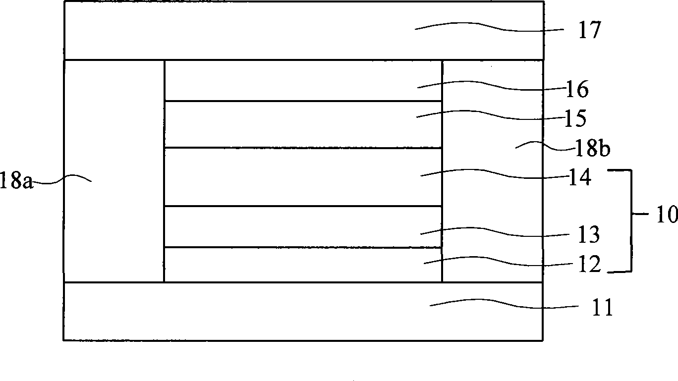
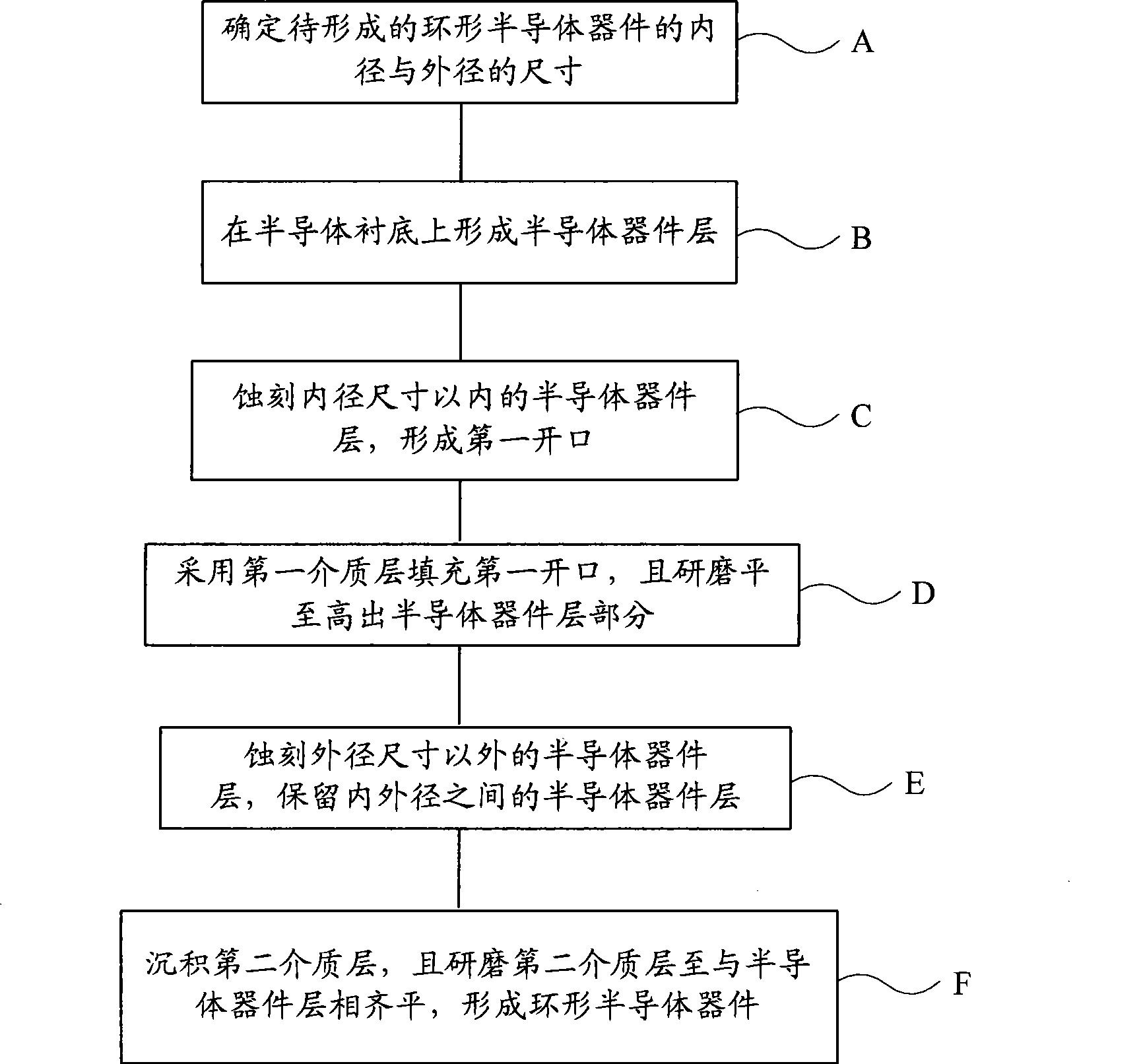
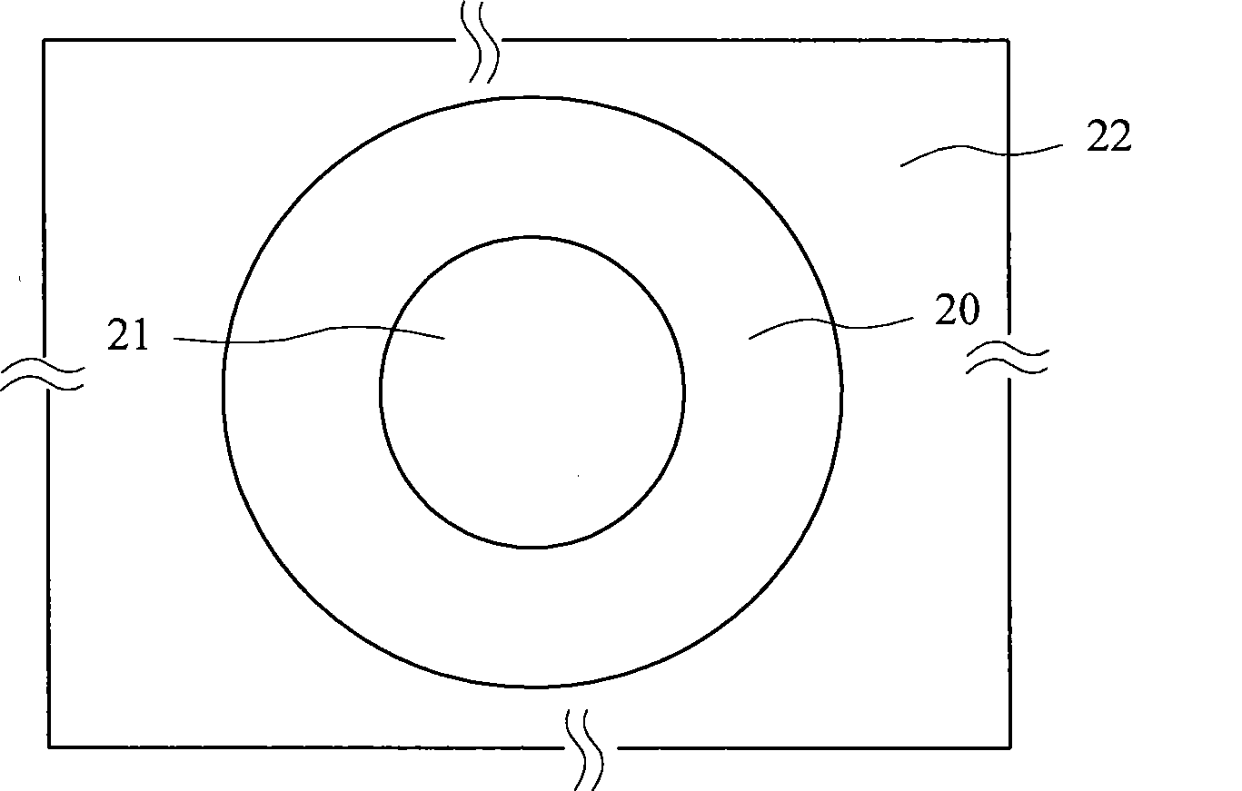
[0044] The present invention provides a ring-shaped semiconductor device and a manufacturing method thereof. The semiconductor device layer within the inner diameter of the ring-shaped semiconductor device is etched first, the first dielectric layer is filled within the inner diameter, and then the part outside the outer diameter of the ring-shaped semiconductor device is removed and the second dielectric layer is deposited. A ring-shaped semiconductor device is formed to achieve the purpose of reducing drive current and reducing power consumption.

[0045] Refer to figure 2 , A schematic flow diagram of a specific embodiment of forming a ring-shaped semiconductor device of the present invention is given. It includes the following steps: performing step A to determine the inner diameter and outer diameter of the ring-shaped semiconductor device to be formed; performing step B to form a semiconductor device layer on the semiconductor substrate; performing step C to etch the semico...


PUM


Abstract

A manufacturing method of a ring-shaped semiconductor device comprises steps of determining sizes of the inner diameter and the outer diameter of a ring-shaped semiconductor device to-be-formed, forming a semiconductor device layer on a semiconductor substrate, removing the semiconductor device layer within the size of the inner diameter to form a first opening, utilizing a first dielectric layer to fill the first opening and flattening the first dielectric layer, removing the semiconductor device layer beyond the size of the outer diameter and maintaining the semiconductor device layer between the inner diameter and the outer diameter, depositing a second dielectric layer and polishing the second dielectric layer until being at the same level with the semiconductor device layer, and finally forming the ring-shape semiconductor device. By firstly etching the inner diameter of the ring-shaped semiconductor device, filling with the first dielectric layer, removing the part beyond the outer diameter of the ring-shaped semiconductor device, depositing the second dielectric layer to fill, the ring-shape semiconductor device is formed, which can realize the purpose of reducing driving current and power consumption.

Description

Technical field [0001] The invention relates to the field of semiconductor devices, in particular to a ring-shaped semiconductor device and a manufacturing method thereof. Background technique [0002] In recent years, with the development of semiconductor technology, semiconductor devices are required to be lighter, thinner, and shorter. It also means that semiconductor devices are developing toward high speed, high integration, and low power consumption. Therefore, the structure of the semiconductor device must be improved to adapt to the development of modern technology. [0003] The following description takes a magnetic random access memory (MRAM) as an example. The structure of the ferromagnetic tunnel junction (hereinafter referred to as MTJ) unit of the existing magnetic random access memory is as follows: figure 1 As shown, it includes a lower electrode layer 11, a lower magnetic layer 10, a tunnel barrier layer 15, and an upper magnetic layer 16 sequentially located on...

Claims


Application Information

Patent Timeline
Patent Type & Authority Applications(China)
IPC IPC(8): H01L43/12H01L43/08H01L21/8246H01L27/22G11C11/16G11C11/15
CPCG11C11/161
Inventor 崔崟
Owner SEMICON MFG INT (SHANGHAI) CORP
Why Eureka
Try Eureka